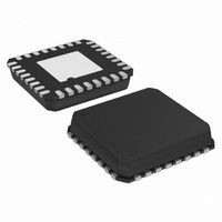
AD8376ACPZ-R7 Analog Devices Inc, AD8376ACPZ-R7 Datasheet - Page 21

AD8376ACPZ-R7
Manufacturer Part Number
AD8376ACPZ-R7
Description
If Cellular Dual DGA
Manufacturer
Analog Devices Inc
Datasheet
1.AD8376ACPZ-R7.pdf
(24 pages)
Specifications of AD8376ACPZ-R7
Design Resources
Using AD8376 to Drive Wide Bandwidth ADCs for High IF AC-Coupled Appls (CN0002) High Performance, Dual Channel IF Sampling Receiver (CN0140)
Amplifier Type
Variable Gain
Number Of Circuits
2
Output Type
Differential
Slew Rate
5000 V/µs
-3db Bandwidth
700MHz
Current - Input Bias
900nA
Current - Supply
250mA
Voltage - Supply, Single/dual (±)
4.5 V ~ 5.5 V
Operating Temperature
-40°C ~ 85°C
Mounting Type
Surface Mount
Package / Case
32-LFCSP
Lead Free Status / RoHS Status
Lead free / RoHS Compliant
Current - Output / Channel
-
Gain Bandwidth Product
-
Voltage - Input Offset
-
Lead Free Status / RoHS Status
Lead free / RoHS Compliant
Other names
AD8376ACPZ-R7TR
Available stocks
Company
Part Number
Manufacturer
Quantity
Price
Company:
Part Number:
AD8376ACPZ-R7
Manufacturer:
Maxim
Quantity:
26
Part Number:
AD8376ACPZ-R7
Manufacturer:
ADI/亚德诺
Quantity:
20 000
Table 6. Evaluation Board Configuration Options
Components
C13, C14, C20 to C22,
C64 to C67, R90, R91
T1, T2, C1 to C4, C61, C62,
R1 to R4, R9 to R12,
R70 to R75
T3, T4, C7 to C10,
L1 to L4, R15 to R32,
R62, R63, C62, C63
PUA, PUB, R13, R14,
C5, C6
WA0 to WA4, WB0 to WB4
C11, C12
Function
Power Supply Decoupling. Nominal supply decoupling consists a
10 μF capacitor to ground followed by 0.1 μF capacitors to ground
positioned as close to the device as possible.
Input Interface. T1 and T2 are 3:1 impedance ratio baluns to
transform a 50 Ω single-ended input into a 150 Ω balanced
differential signal. R1 and R4 ground one side of the differential drive
interface for single-ended applications. R9 to R12 and R70 to R75 are
provided for generic placement of matching components. C1 to C4
are dc blocks.
Output Interface. C7 to C10 are dc blocks. L1 to L4 provide dc biases
for the outputs. R19 to R28 are provided for generic placement of
matching components. The evaluation board is configured to
provide a 150 Ω to 50 Ω impedance transformation with an insertion
loss of about 11 dB. T3 and T4 are 1:1 impedance ratio baluns to
transform the balanced differential signals to single-ended signals.
R29 and R32 ground one side of the differential output interface for
single-ended applications.
Enable Interface. The AD8376 is enabled by applying a logic high
voltage to the ENBA pin for Channel A or the ENBB pin for Channel B.
Channel A is enabled when the PUA switch is set in the up position,
connecting the ENBA pin to VPOS. Likewise, Channel B is enabled
when the PUB switch is set in the up position, connecting the ENBB
pin to VPOS. Both channels are disabled by setting the switches to
the down position, connecting the ENBA and ENBB pins to GND.
Parallel Interface Control. Used to hardwire A0 through A4 and B0
through B4 to the desired gain. The bank of switches WA0 to WA4 set
the binary gain code for Channel A. The bank of switches WB0 to
WB4 set the binary gain code for Channel B. WA0 and WB0 represent
the LSB for each of the respective channels.
Voltage Reference. Input common-mode voltage ac-coupled to
ground by 0.1 μF capacitors, C11 and C12.
Rev. A | Page 21 of 24
Default Conditions
C20 = 10 μF (size 3528)
C13, C14 = 0.1 μF (size 0402)
C21, C22, C64 to C67 = 0.1 μF
(size 0603)
R90, R91 = 0 Ω (size 0603)
T1, T2 = TC3-1+ (Mini-Circuits)
C1 to C4, C60, C61 = 0.1 μF (size 0402)
R1, R4, R9 to R12 = 0 Ω (size 0402)
R2, R3, R70 to R75 = open (size 0402)
C7 to C10 = 0.1 μF (size 0402)
L1 to L4 = 1 μH (size 0805)
T3, T4 = ETC1-1-13 (M/A-COM)
R19 to R22 = 61.9 Ω (size 0402)
R23, R25, R26, R28 = 30.9 Ω (size 0402)
R15 to R18 = 0 Ω (size 0603)
R29, R32 = 0 Ω (size 0402)
R24, R27, R30, R31, R62, R63 = open
(size 0402)
C62, C63 = 0.1 μF (size 0402)
PUA, PUB = installed
R13, R14 = 0 Ω (size 0603)
C5, C6 = open (size 0603)
WA0 to WA4, WB0 to WB4 = installed
C11, C12 = 0.1 μF (size 0402)
AD8376


