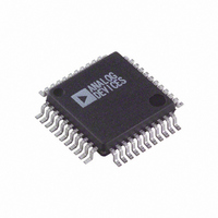
AD9243ASZRL Analog Devices Inc, AD9243ASZRL Datasheet - Page 10

AD9243ASZRL
Manufacturer Part Number
AD9243ASZRL
Description
14-Bit, 3 MSPS Monolithic ADC
Manufacturer
Analog Devices Inc
Datasheet
1.AD9243ASZ.pdf
(24 pages)
Specifications of AD9243ASZRL
Number Of Bits
14
Sampling Rate (per Second)
3M
Data Interface
Parallel
Number Of Converters
7
Power Dissipation (max)
145mW
Voltage Supply Source
Analog and Digital
Operating Temperature
-40°C ~ 85°C
Mounting Type
Surface Mount
Package / Case
44-MQFP, 44-PQFP
Lead Free Status / RoHS Status
Lead free / RoHS Compliant
Available stocks
Company
Part Number
Manufacturer
Quantity
Price
Company:
Part Number:
AD9243ASZRL
Manufacturer:
Analog Devices Inc
Quantity:
10 000
AD9243
Input
Connection
Single-Ended
Single-Ended
Differential
NOTE
1
The optimum size of this resistor is dependent on several factors
which include the AD9243 sampling rate, the selected op amp,
and the particular application. In most applications, a 30
50
quire a larger resistor value to reduce the noise bandwidth or
possibly limit the fault current in an overvoltage condition.
Other applications may require a larger resistor value as part of
an anti-aliasing filter. In any case, since the THD performance
is dependent on the series resistance and the above mentioned
factors, optimizing this resistor value for a given application is
encouraged.
A slight improvement in SNR performance and dc offset perfor-
mance is achieved by matching the input resistance connected
to VINA and VINB. The degree of improvement is dependent on
the resistor value and the sampling rate. For series resistor
values greater than 100 , the use of a matching resistor is
encouraged.
VINA and VINB can be interchanged if signal inversion is required.
Figure 25. Series Resistor Isolates Switched-Capacitor
SHA Input from Op Amp. Matching Resistors Improve
SNR Performance
resistor is sufficient. However, some applications may re-
*OPTIONAL SERIES RESISTOR
V
V
CC
EE
Coupling Span (V)
DC
AC
AC or
DC
10 F
R
S
*
Input
2
2
5
2
2 or
2
5
2
2
2
5
0.1 F
VREF
VREF
VREF
VREF
VREF
R
S
*
VINA
0 to 2
0 to
2
0 to 5
2.5 – VREF
2.5 + VREF
0 to 1 or
0 to 2 VREF
0 to 5
2.5 – VREF
2.5 + VREF
2 to 3
2.5 – VREF/2
2.5 + VREF/2
1.75 to 3.25
VINA
VINB
VREF
SENSE
REFCOM
VREF
AD9243
Table I. Analog Input Configuration Summary
to
to
to
1
Input Range (V)
1
1 or VREF
VINB
VREF
2.5
2.5
2.5
2.5
3 to 2
2.5 + VREF/2
2.5 – VREF/2
3.25 to 1.75
to
1
to
–10–
Figure
#
32, 33
32, 33
32, 33
39
34
34
35
29–31
29–31
29–31
The noise or small-signal bandwidth of the AD9243 is the same
as its full-power bandwidth. For noise sensitive applications, the
excessive bandwidth may be detrimental and the addition of a
series resistor and/or shunt capacitor can help limit the wide-
band noise at the A/D’s input by forming a low-pass filter.
Note, however, that the combination of this series resistance
with the equivalent input capacitance of the AD9243 should be
evaluated for those time-domain applications that are sensitive
to the input signal’s absolute settling time. In applications where
harmonic distortion is not a primary concern, the series resis-
tance may be selected in combination with the SHA’s nominal
16 pF of input capacitance to set the filter’s 3 dB cutoff frequency.
A better method of reducing the noise bandwidth, while possi-
bly establishing a real pole for an antialiasing filter, is to add
some additional shunt capacitance between the input (i.e.,
VINA and/or VINB) and analog ground. Since this additional
shunt capacitance combines with the equivalent input capaci-
tance of the AD9243, a lower series resistance can be selected to
establish the filter’s cutoff frequency while not degrading the
distortion performance of the device. The shunt capacitance
also acts like a charge reservoir, sinking or sourcing the addi-
tional charge required by the hold capacitor, C
ing current transients seen at the op amp’s output.
The effect of this increased capacitive load on the op amp driv-
ing the AD9243 should be evaluated. To optimize performance
when noise is the primary consideration, increase the shunt
capacitance as much as the transient response of the input signal
will allow. Increasing the capacitance too much may adversely
affect the op amp’s settling time, frequency response, and dis-
tortion performance.
Comments
Best for stepped input response applications, suboptimum
THD and noise performance, requires 5 V op amp.
Same as above but with improved noise performance due to
increase in dynamic range. Headroom/settling time require-
ments of
Optimum noise performance, excellent THD performance. Requires
op amp with VCC > +5 V due to insufficient headroom @ 5 V.
Optimum THD performance with VREF = 1, noise performance
improves while THD performance degrades as VREF increases
Suboptimum ac performance due to input common-mode
level not biased at optimum midsupply level (i.e., 2.5 V).
Optimum noise performance, excellent THD performance.
Flexible input range, Optimum THD performance with
VREF = 1. Noise performance improves while THD perfor-
mance degrades as VREF increases to 2.5 V.
Optimum full-scale THD and SFDR performance well be-
yond the A/Ds Nyquist frequency.
Same as 2 V to 3 V input range with the exception that full-scale
THD and SFDR performance can be traded off for better noise
performance.
Widest dynamic range (i.e., ENOBs) due to Optimum Noise
performance.
to 2.5 V. Single supply operation (i.e., +5 V) for many op amps.
5 op amp should be evaluated.
H
, further reduc-
REV. A


