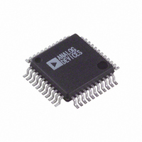
AD9243ASZRL Analog Devices Inc, AD9243ASZRL Datasheet - Page 8

AD9243ASZRL
Manufacturer Part Number
AD9243ASZRL
Description
14-Bit, 3 MSPS Monolithic ADC
Manufacturer
Analog Devices Inc
Datasheet
1.AD9243ASZ.pdf
(24 pages)
Specifications of AD9243ASZRL
Number Of Bits
14
Sampling Rate (per Second)
3M
Data Interface
Parallel
Number Of Converters
7
Power Dissipation (max)
145mW
Voltage Supply Source
Analog and Digital
Operating Temperature
-40°C ~ 85°C
Mounting Type
Surface Mount
Package / Case
44-MQFP, 44-PQFP
Lead Free Status / RoHS Status
Lead free / RoHS Compliant
Available stocks
Company
Part Number
Manufacturer
Quantity
Price
Company:
Part Number:
AD9243ASZRL
Manufacturer:
Analog Devices Inc
Quantity:
10 000
AD9243
INTRODUCTION
The AD9243 utilizes a four-stage pipeline architecture with a
wideband input sample-and-hold amplifier (SHA) implemented
on a cost-effective CMOS process. Each stage of the pipeline,
excluding the last stage, consists of a low resolution flash A/D
connected to a switched capacitor DAC and interstage residue
amplifier (MDAC). The residue amplifier amplifies the differ-
ence between the reconstructed DAC output and the flash input
for the next stage in the pipeline. One bit of redundancy is used
in each of the stages to facilitate digital correction of flash er-
rors. The last stage simply consists of a flash A/D.
The pipeline architecture allows a greater throughput rate at the
expense of pipeline delay or latency. This means that while the
converter is capable of capturing a new input sample every clock
cycle, it actually takes three clock cycles for the conversion to be
fully processed and appear at the output. This latency is not a
concern in most applications. The digital output, together with
the out-of-range indicator (OTR), is latched into an output
buffer to drive the output pins. The output drivers can be con-
figured to interface with +5 V or +3.3 V logic families.
The AD9243 uses both edges of the clock in its internal timing
circuitry (see Figure 1 and specification page for exact timing
requirements). The A/D samples the analog input on the rising
edge of the clock input. During the clock low time (between the
falling edge and rising edge of the clock), the input SHA is in
the sample mode; during the clock high time it is in the hold
mode. System disturbances just prior to the rising edge of the
clock and/or excessive clock jitter may cause the input SHA to
acquire the wrong value, and should be minimized.
ANALOG INPUT AND REFERENCE OVERVIEW
Figure 20, a simplified model of the AD9243, highlights the rela-
tionship between the analog inputs, VINA, VINB, and the
reference voltage, VREF. Like the voltage applied to the top
of the resistor ladder in a flash A/D converter, the value VREF
defines the maximum input voltage to the A/D core. The minimum
input voltage to the A/D core is automatically defined to be –VREF.
Figure 20. AD9243 Equivalent Functional Input Circuit
The addition of a differential input structure gives the user an
additional level of flexibility that is not possible with traditional
flash converters. The input stage allows the user to easily config-
ure the inputs for either single-ended operation or differential
operation. The A/D’s input structure allows the dc offset of the
input signal to be varied independently of the input span of the
converter. Specifically, the input to the A/D core is the difference
of the voltages applied at the VINA and VINB input pins.
VINA
VINB
V
AD9243
CORE
+V
CORE
–V
A/D
REF
REF
14
–8–
Therefore, the equation,
defines the output of the differential input stage and provides the
input to the A/D core.
The voltage, V
where VREF is the voltage at the VREF pin.
While an infinite combination of VINA and VINB inputs exist
that satisfy Equation 2, there is an additional limitation placed
on the inputs by the power supply voltages of the AD9243. The
power supplies bound the valid operating range for VINA and
VINB. The condition,
where AVSS is nominally 0 V and AVDD is nominally +5 V,
defines this requirement. Thus, the range of valid inputs for
VINA and VINB is any combination that satisfies both Equa-
tions 2 and 3.
For additional information showing the relationship between
VINA, VINB, VREF and the digital output of the AD9243, see
Table IV.
Refer to Table I and Table II for a summary of the various
analog input and reference configurations.
ANALOG INPUT OPERATION
Figure 21 shows the equivalent analog input of the AD9243
which consists of a differential sample-and-hold amplifier (SHA).
The differential input structure of the SHA is highly flexible,
allowing the devices to be easily configured for either a differen-
tial or single-ended input. The dc offset, or common-mode
voltage, of the input(s) can be set to accommodate either single-
supply or dual supply systems. Also, note that the analog inputs,
VINA and VINB, are interchangeable with the exception that
reversing the inputs to the VINA and VINB pins results in a
polarity inversion.
VINB
VINA
Figure 21. AD9243 Simplified Input Circuit
CORE
AVSS – 0.3 V < VINA < AVDD + 0.3 V
AVSS – 0.3 V < VINB < AVDD + 0.3 V
, must satisfy the condition,
C
C
C
C
V
–VREF V
PIN
PAR
PIN
PAR
CORE
+
–
Q
Q
= VINA – VINB
S1
S1
CORE
Q
H1
C
C
VREF
S
S
C
C
H
H
Q
Q
S2
S2
REV. A
(2)
(3)
(1)


