AD9778ABSVZ Analog Devices Inc, AD9778ABSVZ Datasheet - Page 42
AD9778ABSVZ
Manufacturer Part Number
AD9778ABSVZ
Description
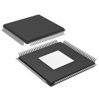
IC,D/A CONVERTER,DUAL,14-BIT,CMOS,TQFP,100PIN
Manufacturer
Analog Devices Inc
Specifications of AD9778ABSVZ
Number Of Bits
14
Data Interface
Parallel
Number Of Converters
2
Voltage Supply Source
Analog and Digital
Power Dissipation (max)
300mW
Operating Temperature
-40°C ~ 85°C
Mounting Type
Surface Mount
Package / Case
100-TQFP Exposed Pad, 100-eTQFP, 100-HTQFP, 100-VQFP
Package
100TQFP EP
Resolution
14 Bit
Conversion Rate
1 GSPS
Architecture
Interpolation Filter
Digital Interface Type
Parallel
Number Of Outputs Per Chip
2
Output Type
Current
Full Scale Error
±2(Typ) %FSR
Integral Nonlinearity Error
±1.5(Typ) LSB
Lead Free Status / RoHS Status
Lead free / RoHS Compliant
For Use With
AD9778A-EBZ - BOARD EVALUATION AD9778A
Settling Time
-
Lead Free Status / RoHS Status
Lead free / RoHS Compliant
Available stocks
Company
Part Number
Manufacturer
Quantity
Price
Company:

Part Number:
AD9778ABSVZ
Manufacturer:
Analog Devices Inc
Quantity:
135
Company:
Part Number:
AD9778ABSVZ
Manufacturer:
Analog Devices Inc
Quantity:
10 000
Part Number:
AD9778ABSVZ
Manufacturer:
ADI/亚德诺
Quantity:
20 000
Company:
Part Number:
AD9778ABSVZRL
Manufacturer:
Analog Devices Inc
Quantity:
10 000


AD9776A/AD9778A/AD9779A
DRIVING THE REFCLK INPUT
The REFCLK input requires a low jitter differential drive signal.
The signal level can range from 400 mV p-p differential to
1.6 V p-p differential centered about a 400 mV input common-
mode voltage. Looking at the single-ended inputs, REFCLK+ or
REFCLK−, each input pin can safely swing from 200 mV p-p to
800 mV p-p about the 400 mV common-mode voltage. Although
these input levels are not directly LVDS compatible, REFCLK
can be driven by an offset ac-coupled LVDS signal, as shown in
Figure 73.
If a clean sine clock is available, it can be transformer-coupled
to REFCLK, as shown in Figure 73. Use of a CMOS or TTL
clock is also acceptable for lower sample rates. It can be routed
through a CMOS to LVDS translator, and then ac-coupled as
described in this section. Alternatively, it can be transformer-
coupled and clamped, as shown in Figure 74.
LVDS_P_IN
LVDS_N_IN
Figure 73. LVDS REFCLK Drive Circuit
0.1µF
0.1µF
50Ω
50Ω
V
CM
= 400mV
REFCLK–
REFCLK+
Rev. B | Page 42 of 56
A simple bias network for generating V
It is important to use CVDD18 and CGND for the clock bias
circuit. Any noise or other signal that is coupled onto the clock
is multiplied by the DAC digital input signal and can degrade
DAC performance.
TTL OR CMOS
CLK INPUT
287Ω
1kΩ
Figure 74. TTL or CMOS REFCLK Drive Circuit
Figure 75. REFCLK V
0.1µF
0.1µF
1nF
CM
Generator Circuit
V
CM
1nF
CM
50Ω
50Ω
= 400mV
is shown in Figure 75.
BAV99ZXCT
HIGH SPEED
DUAL DIODE
V
CM
CVDD18
CGND
= 400mV
REFCLK+
REFCLK–
Related parts for AD9778ABSVZ
Image
Part Number
Description
Manufacturer
Datasheet
Request
R

Part Number:
Description:
Dual 16B, 1.0 GSPS TxDAC
Manufacturer:
Analog Devices Inc
Datasheet:
Part Number:
Description:
BOARD EVALUATION FOR AD9778
Manufacturer:
Analog Devices Inc
Datasheet:

Part Number:
Description:
±1.7g Dual-Axis IMEMS Accelerometer Evaluation Board
Manufacturer:
Analog Devices Inc
Datasheet:
Part Number:
Description:
Inertial Sensor Evaluation System
Manufacturer:
Analog Devices Inc
Datasheet:
Part Number:
Description:
Manufacturer:
Analog Devices Inc
Datasheet:
Part Number:
Description:
Manufacturer:
Analog Devices Inc
Datasheet:
Part Number:
Description:
Manufacturer:
Analog Devices Inc
Datasheet:
Part Number:
Description:
Manufacturer:
Analog Devices Inc
Datasheet:
Part Number:
Description:
Manufacturer:
Analog Devices Inc
Datasheet:
Part Number:
Description:
Manufacturer:
Analog Devices Inc
Datasheet:
Part Number:
Description:
Manufacturer:
Analog Devices Inc
Datasheet:
Part Number:
Description:
Manufacturer:
Analog Devices Inc
Datasheet: