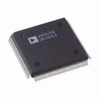
AD9887AKSZ-140 Analog Devices Inc, AD9887AKSZ-140 Datasheet - Page 15

AD9887AKSZ-140
Manufacturer Part Number
AD9887AKSZ-140
Description
IC,TV/VIDEO CIRCUIT,Video Digitizer,CMOS,QFP,160PIN,PLASTIC
Manufacturer
Analog Devices Inc
Datasheet
1.AD9887AKSZ-140.pdf
(52 pages)
Specifications of AD9887AKSZ-140
Applications
Graphic Cards, VGA Interfaces
Interface
Analog and Digital
Voltage - Supply
3.15 V ~ 3.45 V
Package / Case
160-MQFP, 160-PQFP
Mounting Type
Surface Mount
Lead Free Status / RoHS Status
Lead free / RoHS Compliant
Available stocks
Company
Part Number
Manufacturer
Quantity
Price
Company:
Part Number:
AD9887AKSZ-140
Manufacturer:
MAX
Quantity:
59
Company:
Part Number:
AD9887AKSZ-140
Manufacturer:
ADI
Quantity:
364
Company:
Part Number:
AD9887AKSZ-140
Manufacturer:
Analog Devices Inc
Quantity:
10 000
Part Number:
AD9887AKSZ-140
Manufacturer:
ADI/亚德诺
Quantity:
20 000
R
G
B
R
G
B
MIDSC
CLAMP
MIDSC
CLAMP
MIDSC
CLAMP
V
V
V
V
V
V
Red Channel Midscale Clamp Voltage Output
Green Channel Midscale Clamp Voltage Output
Blue Channel Midscale Clamp Voltage Output
Red Channel Midscale Clamp Voltage Input
Green Channel Midscale Clamp Voltage Input
Blue Channel Midscale Clamp Voltage Input
These pins are part of the circuit that provides a
voltage reference for midscale clamping used in the
capture of YUV and YPbPr input signals. These
pins should be grounded through 0.1 μF capacitors,
as shown in Figure 4.
Rev. B | Page 15 of 52
Data Clock Outputs
DATACK Data Output Clock
DATACK Data Output Clock Complement
These signals are produced by the internal clock
generator and are synchronous with the internal
pixel sampling clock.
When the AD9887A is operated in single-channel
mode, the output frequency is equal to the pixel
sampling frequency. When the AD9887A is operated
in dual-channel mode, the clock frequency is half
the pixel frequency.
When the sampling time is changed by adjusting
the PHASE register, the output timing is shifted as
well. The Data, DATACK, DATACK , and HSOUT
outputs are moved; therefore, the timing
relationship among the signals is maintained.
These differential data clock output signals are used to
strobe the output data and HSOUT into external logic.
AD9887A


