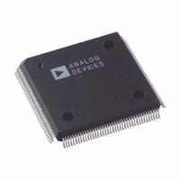
AD9887AKSZ-140 Analog Devices Inc, AD9887AKSZ-140 Datasheet - Page 50

AD9887AKSZ-140
Manufacturer Part Number
AD9887AKSZ-140
Description
IC,TV/VIDEO CIRCUIT,Video Digitizer,CMOS,QFP,160PIN,PLASTIC
Manufacturer
Analog Devices Inc
Datasheet
1.AD9887AKSZ-140.pdf
(52 pages)
Specifications of AD9887AKSZ-140
Applications
Graphic Cards, VGA Interfaces
Interface
Analog and Digital
Voltage - Supply
3.15 V ~ 3.45 V
Package / Case
160-MQFP, 160-PQFP
Mounting Type
Surface Mount
Lead Free Status / RoHS Status
Lead free / RoHS Compliant
Available stocks
Company
Part Number
Manufacturer
Quantity
Price
Company:
Part Number:
AD9887AKSZ-140
Manufacturer:
MAX
Quantity:
59
Company:
Part Number:
AD9887AKSZ-140
Manufacturer:
ADI
Quantity:
364
Company:
Part Number:
AD9887AKSZ-140
Manufacturer:
Analog Devices Inc
Quantity:
10 000
Part Number:
AD9887AKSZ-140
Manufacturer:
ADI/亚德诺
Quantity:
20 000
AD9887A
PLL
Place the PLL loop filter components as close as possible to the
FILT pin. Do not place any digital or other high frequency
traces near these components. Use the values suggested in the
Specifications section with 10% tolerances or less.
OUTPUTS—BOTH DATA AND CLOCKS
Try to minimize the trace length that the digital outputs must
drive. Longer traces have higher capacitance, requiring more
current and causing more internal digital noise. Shorter traces
reduce the possibility of reflections.
Adding a series resistor with a value of 22 Ω to 100 Ω can suppress
reflections, reduce EMI, and reduce the current spikes inside of
the AD9887A. However, if 50 Ω traces are used on the PCB, the
data outputs should not need these resistors. A 22 Ω resistor on
the DATACK output should provide good impedance matching
that further reduces reflections. If EMI or current spiking is a
concern, it is recommended to use a lower drive strength setting.
If series resistors are used, place them as close as possible to the
AD9887A pins, but try not to add vias or extra length to the
output trace.
If possible, limit the capacitance that each of the digital outputs
drives to less than 10 pF. This can be accomplished easily by
Rev. B | Page 50 of 52
keeping traces short and connecting the outputs to only one
device. Loading the outputs with excessive capacitance increases
the current transients inside the AD9887A, creating digital
noise on the power supplies.
DIGITAL INPUTS
The digital inputs on the AD9887A are designed to work with
3.3 V signals.
Any noise in the HSYNC input trace produces jitter in the
system. Therefore, minimize the trace length and do not run
any digital or other high frequency traces near it.
VOLTAGE REFERENCE
The voltage reference should be bypassed with a 0.1 μF
capacitor. Place it as close as possible to the AD9887A pin.
Make the ground connection as short as possible.
REFOUT is easily connected to REFIN with a short trace.
Avoid making this trace longer than necessary.
When using an external reference, the REFOUT output,
although unused, still needs to be bypassed with a 0.1 μF
capacitor to avoid ringing.


