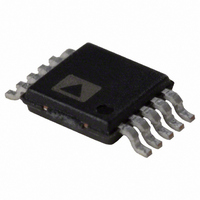
ADA4310-1ARHZ-R7 Analog Devices Inc, ADA4310-1ARHZ-R7 Datasheet - Page 12

ADA4310-1ARHZ-R7
Manufacturer Part Number
ADA4310-1ARHZ-R7
Description
IC,Operational Amplifier,DUAL,BIPOLAR,TSSOP,10PIN,PLASTIC
Manufacturer
Analog Devices Inc
Datasheet
1.ADA4310-1ACPZ-R7.pdf
(16 pages)
Specifications of ADA4310-1ARHZ-R7
Amplifier Type
Current Feedback
Number Of Circuits
2
Slew Rate
820 V/µs
-3db Bandwidth
190MHz
Current - Input Bias
6µA
Voltage - Input Offset
1000µV
Current - Supply
7.6mA
Voltage - Supply, Single/dual (±)
5 V ~ 12 V, ±2.5 V ~ 6 V
Operating Temperature
-40°C ~ 85°C
Mounting Type
Surface Mount
Package / Case
10-MSOP, Micro10™, 10-uMAX, 10-uSOP
Lead Free Status / RoHS Status
Lead free / RoHS Compliant
Output Type
-
Current - Output / Channel
-
Gain Bandwidth Product
-
Lead Free Status / RoHS Status
Lead free / RoHS Compliant
ADA4310-1
BOARD LAYOUT
As is the case with all high speed applications, careful attention
to printed circuit board layout details prevents associated board
parasitics from becoming problematic. Proper RF design
technique is mandatory. The PCB should have a ground plane
covering all unused portions of the component side of the
board to provide a low impedance return path. Removing the
ground plane on all layers from the area near the input and
output pins reduces stray capacitance, particularly in the area of
the inverting inputs. Signal lines connecting the feedback and
gain resistors should be as short as possible to minimize the
inductance and stray capacitance associated with these traces.
Termination resistors and loads should be located as close as
possible to their respective inputs and outputs. Input and output
traces should be kept as far apart as possible to minimize
coupling (crosstalk) though the board. Wherever there are
complementary signals, a symmetrical layout should be
provided to the extent possible to maximize balanced
performance. When running differential signals over a long
distance, the traces on the PCB should be close. This reduces
the radiated energy and makes the circuit less susceptible to RF
interference. Adherence to stripline design techniques for long
signal traces (greater than about 1 inch) is recommended.
For more information on high speed board layout, go to
www.analog.com
Circuit-Board Layout.
and A Practical Guide to High-Speed Printed-
Rev. 0 | Page 12 of 16
POWER SUPPLY BYPASSING
The ADA4310-1 operates on supplies, from +5 V to ±6 V. The
ADA4310-1 circuit should be powered with a well-regulated
power supply. Careful attention must be paid to decoupling the
power supply. High quality capacitors with low equivalent series
resistance (ESR), such as multilayer ceramic capacitors
(MLCCs), should be used to minimize supply voltage ripple and
power dissipation. In addition, 0.1 μF MLCC decoupling
capacitors should be located no more than ⅛-inch away from
each of the power supply pins. A large, usually tantalum, 10 μF
capacitor is required to provide good decoupling for lower
frequency signals and to supply current for fast, large signal
changes at the ADA4310-1 outputs. Bypassing capacitors should
be laid out in such a manner to keep return currents away from
the inputs of the amplifiers. This minimizes any voltage drops
that can develop due to ground currents flowing through the
ground plane. A large ground plane also provides a low
impedance path for the return currents.


