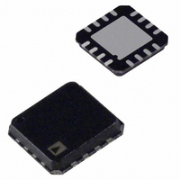
ADA4939-1YCPZ-R7 Analog Devices Inc, ADA4939-1YCPZ-R7 Datasheet - Page 17

ADA4939-1YCPZ-R7
Manufacturer Part Number
ADA4939-1YCPZ-R7
Description
IC,Differential Amplifier,SINGLE,BIPOLAR,LLCC,16PIN,PLASTIC
Manufacturer
Analog Devices Inc
Type
Differential ADC Driverr
Datasheet
1.ADA4939-1YCPZ-R7.pdf
(24 pages)
Specifications of ADA4939-1YCPZ-R7
Amplifier Type
Differential
Number Of Circuits
1
Output Type
Differential
Slew Rate
6800 V/µs
-3db Bandwidth
1.4GHz
Current - Input Bias
10µA
Voltage - Input Offset
500µV
Current - Supply
36.5mA
Current - Output / Channel
100mA
Voltage - Supply, Single/dual (±)
3 V ~ 5.25 V, ±1.5 V ~ 2.625 V
Operating Temperature
-40°C ~ 105°C
Mounting Type
Surface Mount
Package / Case
16-LFCSP
Number Of Channels
1
Number Of Elements
1
Power Supply Requirement
Single
Common Mode Rejection Ratio
77dB
Input Resistance
0.45MOhm
Input Offset Voltage
2.8mV
Input Bias Current
2.2uA
Single Supply Voltage (typ)
5V
Dual Supply Voltage (typ)
Not RequiredV
Power Supply Rejection Ratio
80dB
Rail/rail I/o Type
No
Single Supply Voltage (min)
3V
Single Supply Voltage (max)
5.25V
Dual Supply Voltage (min)
Not RequiredV
Dual Supply Voltage (max)
Not RequiredV
Operating Temp Range
-40C to 105C
Operating Temperature Classification
Industrial
Mounting
Surface Mount
Pin Count
16
Package Type
LFCSP EP
Lead Free Status / RoHS Status
Lead free / RoHS Compliant
Gain Bandwidth Product
-
Lead Free Status / Rohs Status
Compliant
Other names
ADA4939-1YCPZ-R7TR
Available stocks
Company
Part Number
Manufacturer
Quantity
Price
Company:
Part Number:
ADA4939-1YCPZ-R7
Manufacturer:
Analog Devices Inc
Quantity:
1 948
THEORY OF OPERATION
The ADA4939 differs from conventional op amps in that it has
two outputs whose voltages move in opposite directions and an
additional input, V
loop gain and negative feedback to force these outputs to the
desired voltages. The ADA4939 behaves much like a standard
voltage feedback op amp and facilitates single-ended-to-differential
conversions, common-mode level shifting, and amplifications of
differential signals. Like an op amp, the ADA4939 has high input
impedance and low output impedance. Because it uses voltage
feedback, the ADA4939 manifests a nominally constant gain-
bandwidth product.
Two feedback loops are employed to control the differential and
common-mode output voltages. The differential feedback, set
with external resistors, controls only the differential output voltage.
The common-mode feedback controls only the common-mode
output voltage. This architecture makes it easy to set the output
common-mode level to any arbitrary value within the specified
limits. The output common-mode voltage is forced, by the internal
common-mode feedback loop, to be equal to the voltage applied
to the V
The internal common-mode feedback loop produces outputs
that are highly balanced over a wide frequency range without
requiring tightly matched external components. This results in
differential outputs that are very close to the ideal of being
identical in amplitude and are exactly 180° apart in phase.
ANALYZING AN APPLICATION CIRCUIT
The ADA4939 uses high open-loop gain and negative feedback
to force its differential and common-mode output voltages in
such a way as to minimize the differential and common-mode
error voltages. The differential error voltage is defined as the
voltage between the differential inputs labeled +IN and −IN
(see Figure 42). For most purposes, this voltage can be assumed
to be zero. Similarly, the difference between the actual output
common-mode voltage and the voltage applied to V
be assumed to be zero. Starting from these two assumptions,
any application circuit can be analyzed.
OCM
input.
OCM
. Like an op amp, it relies on high open-
OCM
can also
Rev. 0 | Page 17 of 24
SETTING THE CLOSED-LOOP GAIN
The differential-mode gain of the circuit in Figure 42 can be
determined by
This presumes that the input resistors (R
(R
STABLE FOR GAINS ≥2
The ADA4939 frequency response exhibits excessive peaking
for differential gains <2; therefore, the part should be operated
with differential gains ≥2.
ESTIMATING THE OUTPUT NOISE VOLTAGE
The differential output noise of the ADA4939 can be estimated
using the noise model in Figure 43. The input-referred noise
voltage density, v
noise currents, i
ground. The output voltage due to v
v
follows). The noise currents are uncorrelated with the same
mean-square value, and each produces an output voltage that is
equal to the noise current multiplied by the associated feedback
resistance. The noise voltage density at the V
When the feedback networks have the same feedback factor, as
in most cases, the output noise due to v
Each of the four resistors contributes (4kTR
from the feedback resistors appears directly at the output, and
the noise from the gain resistors appears at the output multiplied
by R
multiplication factors, and the output-referred noise density terms.
nIN
F
) on each side are equal.
by the noise gain, G
F
/R
V
V
OUT
G
IN
. Table 11 summarizes the input noise sources, the
,
,
dm
dm
V
V
nRG1
nRG2
=
nIN−
R
R
nIN
R
R
G
F
i
i
G1
G2
, is modeled as a differential input, and the
nIN+
nIN–
and i
Figure 43. Noise Model
N
nIN+
(defined in the G
V
nIN
ADA4939-1/ADA4939-2
, appear between each input and
R
R
F1
F2
ADA4939
+
nIN
V
V
V
nRF1
OCM
nRF2
is obtained by multiplying
G
nCM
) and feedback resistors
N
is common-mode.
xx
equation that
V
OCM
)
nOD
1/2
V
nCM
. The noise
pin is v
nCM
.


