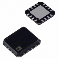
ADA4939-1YCPZ-R7 Analog Devices Inc, ADA4939-1YCPZ-R7 Datasheet - Page 20

ADA4939-1YCPZ-R7
Manufacturer Part Number
ADA4939-1YCPZ-R7
Description
IC,Differential Amplifier,SINGLE,BIPOLAR,LLCC,16PIN,PLASTIC
Manufacturer
Analog Devices Inc
Type
Differential ADC Driverr
Datasheet
1.ADA4939-1YCPZ-R7.pdf
(24 pages)
Specifications of ADA4939-1YCPZ-R7
Amplifier Type
Differential
Number Of Circuits
1
Output Type
Differential
Slew Rate
6800 V/µs
-3db Bandwidth
1.4GHz
Current - Input Bias
10µA
Voltage - Input Offset
500µV
Current - Supply
36.5mA
Current - Output / Channel
100mA
Voltage - Supply, Single/dual (±)
3 V ~ 5.25 V, ±1.5 V ~ 2.625 V
Operating Temperature
-40°C ~ 105°C
Mounting Type
Surface Mount
Package / Case
16-LFCSP
Number Of Channels
1
Number Of Elements
1
Power Supply Requirement
Single
Common Mode Rejection Ratio
77dB
Input Resistance
0.45MOhm
Input Offset Voltage
2.8mV
Input Bias Current
2.2uA
Single Supply Voltage (typ)
5V
Dual Supply Voltage (typ)
Not RequiredV
Power Supply Rejection Ratio
80dB
Rail/rail I/o Type
No
Single Supply Voltage (min)
3V
Single Supply Voltage (max)
5.25V
Dual Supply Voltage (min)
Not RequiredV
Dual Supply Voltage (max)
Not RequiredV
Operating Temp Range
-40C to 105C
Operating Temperature Classification
Industrial
Mounting
Surface Mount
Pin Count
16
Package Type
LFCSP EP
Lead Free Status / RoHS Status
Lead free / RoHS Compliant
Gain Bandwidth Product
-
Lead Free Status / Rohs Status
Compliant
Other names
ADA4939-1YCPZ-R7TR
Available stocks
Company
Part Number
Manufacturer
Quantity
Price
Company:
Part Number:
ADA4939-1YCPZ-R7
Manufacturer:
Analog Devices Inc
Quantity:
1 948
ADA4939-1/ADA4939-2
2.
3.
2V p-p
V
1.09V p-p
S
It can be seen from Figure 47 that the effective R
upper feedback loop is now greater than the R
lower loop due to the addition of the termination resistors.
To compensate for the imbalance of the gain resistors,
a correction resistor (R
lower loop. R
source resistance R
is equal to R
R
1 V p-p, which was obtained with R
circuit with the Thevenin equivalent of the terminated source
and R
Figure 49 presents a tractable circuit with matched
feedback loops that can be easily evaluated.
In order to match the 50 Ω source resistance, the termi-
nation resistor, R
The closest standard 1% value for R
TS
Figure 49. Thevenin Equivalent and Matched Gain Resistors
V
= R
50Ω
R
TH
S
TS
2V p-p
TH
Figure 48. Calculating the Thevenin Equivalent
in the lower feedback loop is shown in Figure 49.
50Ω
R
V
= R
Figure 47. Adding Termination Resistor R
27.4Ω
27.4Ω
IN
S
R
60.4Ω
R
S
TH
||R
TS
TS
S
||R
R
50Ω
is equal to the Thevenin equivalent of the
T
R
T
S
.
T
T
200Ω
V
200Ω
, is calculated using R
R
R
= 27.4 Ω. Note that V
OCM
S
G
G
and the termination resistance R
200Ω
200Ω
V
R
R
OCM
R
60.4Ω
G
G
T
TS
) is added in series with R
400Ω
400Ω
ADA4939
R
R
F
F
+V
–V
400Ω
ADA4939
400Ω
1.09V p-p
R
R
S
S
F
F
+V
–V
S
S
V
T
T
TH
= 50 Ω. The modified
is 60.4 Ω.
T
TH
||300 Ω = 50 Ω.
27.4Ω
R
is greater than
TH
T
R
L
G
R
in the
V
L
G
OUT, dm
in the
G
V
in the
OUT, dm
T
and
Rev. 0 | Page 20 of 24
4.
2V p-p
Figure 50. Terminated Single-Ended-to-Differential System with G = 2
It is useful to point out two effects that occur with a
terminated input. The first is that the value of R
in both loops, lowering the overall closed-loop gain. The
second is that V
be if R
the output voltage, and for large resistor values in the feedback
loops (~1 kΩ), the effects essentially cancel each other out.
For small R
gain is not canceled completely by the increased V
can be seen by evaluating Figure 49.
The desired differential output in this example is 2 V p-p
because the terminated input signal was 1 V p-p and the
closed-loop gain = 2. The actual differential output voltage,
however, is equal to (1.09 V p-p)(400/227.4) = 1.92 V p-p.
To obtain the desired output voltage of 2 V p-p, a final gain
adjustment can be made by increasing R
any of the input circuitry. This is discussed in Step 4.
The feedback resistor value is modified as a final gain
adjustment to obtain the desired output voltage.
To make the output voltage V
calculated using the following formula:
The closest standard 1 % values to 417 Ω are 412 Ω and
422 Ω. Choosing 422 Ω gives a differential output voltage
of 2.02 V p-p.
The final circuit is shown in Figure 50.
R
V
(
F
Desired
S
=
50Ω
T
R
S
= 50 Ω. These two effects have opposite impacts on
V
F
OUT
1V p-p
60.4Ω
and R
V
27.4Ω
TH
R
R
,
dm
TS
T
TH
) (
is a little larger than 1 V p-p, as it would
G
R
, however, the diminished closed-loop
200Ω
200Ω
V
G
R
R
OCM
G
G
+
R
TS
) (
=
OUT
422Ω
422Ω
ADA4939
R
R
2
F
F
+V
–V
= 2 V p-p, R
V
. 1
P
S
S
−
09
P
F
)(
V
without modifying
227
P
−
P
4 .
G
Ω
F
is increased
must be
R
)
L
=
TH
V
2.02V p-p
417
OUT, dm
. This
Ω


