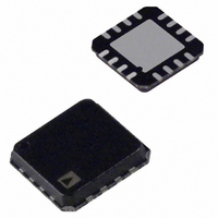
ADA4939-1YCPZ-R7 Analog Devices Inc, ADA4939-1YCPZ-R7 Datasheet - Page 3

ADA4939-1YCPZ-R7
Manufacturer Part Number
ADA4939-1YCPZ-R7
Description
IC,Differential Amplifier,SINGLE,BIPOLAR,LLCC,16PIN,PLASTIC
Manufacturer
Analog Devices Inc
Type
Differential ADC Driverr
Datasheet
1.ADA4939-1YCPZ-R7.pdf
(24 pages)
Specifications of ADA4939-1YCPZ-R7
Amplifier Type
Differential
Number Of Circuits
1
Output Type
Differential
Slew Rate
6800 V/µs
-3db Bandwidth
1.4GHz
Current - Input Bias
10µA
Voltage - Input Offset
500µV
Current - Supply
36.5mA
Current - Output / Channel
100mA
Voltage - Supply, Single/dual (±)
3 V ~ 5.25 V, ±1.5 V ~ 2.625 V
Operating Temperature
-40°C ~ 105°C
Mounting Type
Surface Mount
Package / Case
16-LFCSP
Number Of Channels
1
Number Of Elements
1
Power Supply Requirement
Single
Common Mode Rejection Ratio
77dB
Input Resistance
0.45MOhm
Input Offset Voltage
2.8mV
Input Bias Current
2.2uA
Single Supply Voltage (typ)
5V
Dual Supply Voltage (typ)
Not RequiredV
Power Supply Rejection Ratio
80dB
Rail/rail I/o Type
No
Single Supply Voltage (min)
3V
Single Supply Voltage (max)
5.25V
Dual Supply Voltage (min)
Not RequiredV
Dual Supply Voltage (max)
Not RequiredV
Operating Temp Range
-40C to 105C
Operating Temperature Classification
Industrial
Mounting
Surface Mount
Pin Count
16
Package Type
LFCSP EP
Lead Free Status / RoHS Status
Lead free / RoHS Compliant
Gain Bandwidth Product
-
Lead Free Status / Rohs Status
Compliant
Other names
ADA4939-1YCPZ-R7TR
Available stocks
Company
Part Number
Manufacturer
Quantity
Price
Company:
Part Number:
ADA4939-1YCPZ-R7
Manufacturer:
Analog Devices Inc
Quantity:
1 948
SPECIFICATIONS
5 V OPERATION
T
All specifications refer to single-ended input and differential outputs, unless otherwise noted. Refer to Figure 42 for signal definitions.
±D
Table 1.
Parameter
DYNAMIC PERFORMANCE
NOISE/HARMONIC PERFORMANCE
INPUT CHARACTERISTICS
OUTPUT CHARACTERISTICS
A
Second Harmonic
Third Harmonic
IMD
Voltage Noise (RTI)
Input Current Noise
Crosstalk
Offset Voltage
Input Bias Current
Input Offset Current
Input Resistance
Input Capacitance
Input Common-Mode Voltage
CMRR
Output Voltage Swing
Linear Output Current
Output Balance Error
−3 dB Small Signal Bandwidth
Bandwidth for 0.1 dB Flatness
Large Signal Bandwidth
Slew Rate
Overdrive Recovery Time
= 25°C, +V
IN
to V
OUT, dm
S
= 5 V, −V
Performance
S
= 0 V, V
OCM
= +V
f = 100 kHz
Conditions
V
V
V
V
V
V
See Figure 41 for distortion test circuit
V
V
V
V
V
V
f
f
f = 100 kHz
f = 100 MHz, ADA4939-2
V
T
T
Differential
Common mode
∆V
Maximum ∆V
∆V
see Figure 40 for test circuit
1
1
MIN
MIN
OUT, dm
OUT, dm
OUT, dm
OUT, dm
OUT, dm
IN
OUT, dm
OUT, dm
OUT, dm
OUT, dm
OUT, dm
OUT, dm
OS, dm
= 70 MHz, f
= 140 MHz, f
OUT, dm
OUT, cm
= 0 V to 1.5 V step, G = 3.16
S
/2, R
to T
to T
= V
= 0.1 V p-p
= 0.1 V p-p, ADA4939-1
= 0.1 V p-p, ADA4939-2
= 2 V p-p
= 2 V p-p, 25% to 75%
= 2 V p-p, 10 MHz
= 2 V p-p, 70 MHz
= 2 V p-p, 100 MHz
= 2 V p-p, 10 MHz
= 2 V p-p, 70 MHz
= 2 V p-p, 100 MHz
/∆V
MAX
MAX
/∆V
F
OUT, dm
= 402 Ω, R
variation
variation
OUT, dm
IN, cm
2
OUT
2
= 70.1 MHz, V
/2, V
, ∆V
= 140.1 MHz, V
; single-ended output, R
, ∆V
DIN+
IN, cm
OUT, dm
Rev. 0 | Page 3 of 24
G
= 200 Ω, R
= V
= ±1 V
DIN−
= 1 V, 10 MHz,
OUT, dm
= 2.5 V
OUT, dm
T
= 2 V p-p
= 60.4 Ω (when used), R
= 2 V p-p
F
= R
G
= 10 kΩ
L, dm
ADA4939-1/ADA4939-2
Min
−3.4
−26
−11.2
1.1
0.9
= 1 kΩ, unless otherwise noted.
Typ
1400
300
90
1400
6800
<1
−102
−83
−77
−101
−97
−91
−95
−89
2.3
6
−80
±0.5
±2.0
−10
±0.5
+0.5
180
450
1
−83
100
−64
Max
+2.8
+2.2
+11.2
3.9
−77
4.1
Unit
MHz
MHz
MHz
MHz
V/μs
ns
dBc
dBc
dBc
dBc
dBc
dBc
dBc
dBc
nV/√Hz
pA/√Hz
dB
mV
μV/°C
μA
μA/°C
μA
kΩ
kΩ
pF
V
dB
V
mA
dB


