ADADC85-12 Analog Devices Inc, ADADC85-12 Datasheet - Page 8
ADADC85-12
Manufacturer Part Number
ADADC85-12
Description
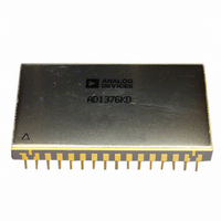
IC,A/D CONVERTER,SINGLE,12-BIT,HYBRID,DIP,32PIN
Manufacturer
Analog Devices Inc
Datasheet
1.ADADC85-12.pdf
(12 pages)
Specifications of ADADC85-12
Rohs Status
RoHS non-compliant
Number Of Bits
12
Sampling Rate (per Second)
100k
Data Interface
Parallel
Number Of Converters
1
Voltage Supply Source
Dual ±
Operating Temperature
-55°C ~ 125°C
Mounting Type
Through Hole
Package / Case
32-CDIP (0.900", 22.86mm)
Lead Free Status / RoHS Status
Available stocks
Company
Part Number
Manufacturer
Quantity
Price


AD ADC84/AD ADC85
INPUT SCALING
The AD ADC84/AD ADC85 inputs should be scaled as close to
the maximum input signal range as possible in order to utilize
the maximum signal resolution of the A/D converter. Connect
the input signal as shown in Table 3. See Figure 11 for circuit
detail.
Table 2. Short Cycle Connections
Connect Short Cycle
Pin 14 to Pin
16
2
4
Table 3. Input Scaling Connections
Input Signal Range
±10 V
±5 V
±2.5 V
0 V to +5 V
0 V to +10 V
INPUT VOLTAGE RANGE AND LSB VALUES
Table 4. Input Voltages and Code Definition
Analog Input Voltage Range
Code Designation
One Least Significant Bit (LSB)
Transition Values
MSB
000 . . . 000
011 . . . 111
111 . . . 110
1
2
3
4
COB = Complementary Offset Binary.
CTC = Complementary Twos Complement – obtained by using the complement of the most significant bit ( MSB ). MSB is available to Pin 13.
CSB = Complementary Straight Binary.
Voltages given are the nominal value for transition to the code specified.
4
LSB
Output Code
COB or CTC
COB or CTC
COB or CTC
CSB
CSB
Connect Clock Rate Control
Pin 17 to Pin
15
16
28
n = 8
n = 10
n = 12
+Full Scale
Mid Scale
–Full Scale
FSR
2
n
Connect Pin 23 to Pin
22
22
22
26
26
±10 V
COB
78.13 mV
19.53 mV
4.88 mV
+10 V –3/2 LSB
0
–10 V +1/2 LSB
20V
2
n
1
or CTC
Bits
12
10
8
Rev. B | Page 8 of 12
2
Connect Pin 25 to
Input Signal
Open
Pin 22
Pin 22
Open
Resolution
(% FSR)
0.024
0.100
0.390
±5 V
COB or CTC
39.06 mV
9.77 mV
2.44 mV
+5 V –3/2 LSB
0
–5 V +1/2 LSB
10V
2
n
±2.5 V
COB or CTC
19.53 mV
4.88 mV
1.22 mV
+2.5 –3/2 LSB
0
–2.5 V +1/2 LSB
5V
AD ADC84/AD ADC85
ConversionTime (μs)
10 (5)
8.5 (4.1)
6.8 (3.3)
2
For Direct Input Connect
Input Signal to Pin
25
24
24
24
24
n
Figure 11. Input Scaling Circuit
0 V to +10 V
CSB
39.06 mV
9.77 mV
2.44 mV
+10 V –3/2 LSB
+5 V
0 V +1/2 LSB
10V
2
n
3
Input Pin 30 Connect
Pin 29 to Pin
25
24
24
24
24
Status Flag
Reset
t
t
t
0 V to +5 V
CSB
19.53 mV
4.88 mV
1.22 mV
+5 V –3/2 LSB
+2.5 V
0 V +1/2 LSB
12
10
8
5V
2
+ 40 ns
n
+ 40 ns
+ 40 ns
Related parts for ADADC85-12
Image
Part Number
Description
Manufacturer
Datasheet
Request
R

Part Number:
Description:
±1.7g Dual-Axis IMEMS Accelerometer Evaluation Board
Manufacturer:
Analog Devices Inc
Datasheet:

Part Number:
Description:
Inertial Sensor Evaluation System
Manufacturer:
Analog Devices Inc
Datasheet:
Part Number:
Description:
Manufacturer:
Analog Devices Inc
Datasheet:
Part Number:
Description:
Manufacturer:
Analog Devices Inc
Datasheet:
Part Number:
Description:
Manufacturer:
Analog Devices Inc
Datasheet:
Part Number:
Description:
Manufacturer:
Analog Devices Inc
Datasheet:
Part Number:
Description:
Manufacturer:
Analog Devices Inc
Datasheet:
Part Number:
Description:
Manufacturer:
Analog Devices Inc
Datasheet:
Part Number:
Description:
Manufacturer:
Analog Devices Inc
Datasheet:
Part Number:
Description:
Manufacturer:
Analog Devices Inc
Datasheet:
Part Number:
Description:
Manufacturer:
Analog Devices Inc
Datasheet:
Part Number:
Description:
Manufacturer:
Analog Devices Inc
Datasheet:
Part Number:
Description:
Manufacturer:
Analog Devices Inc
Datasheet: