ADADC85-12 Analog Devices Inc, ADADC85-12 Datasheet - Page 9
ADADC85-12
Manufacturer Part Number
ADADC85-12
Description
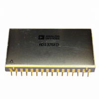
IC,A/D CONVERTER,SINGLE,12-BIT,HYBRID,DIP,32PIN
Manufacturer
Analog Devices Inc
Datasheet
1.ADADC85-12.pdf
(12 pages)
Specifications of ADADC85-12
Rohs Status
RoHS non-compliant
Number Of Bits
12
Sampling Rate (per Second)
100k
Data Interface
Parallel
Number Of Converters
1
Voltage Supply Source
Dual ±
Operating Temperature
-55°C ~ 125°C
Mounting Type
Through Hole
Package / Case
32-CDIP (0.900", 22.86mm)
Lead Free Status / RoHS Status
Available stocks
Company
Part Number
Manufacturer
Quantity
Price


CALIBRATION
External ZERO ADJ and GAIN ADJ potentiometers, connected
as shown in Figure 12 and Figure 13, are used for device
calibration. To prevent interaction of these two adjustments,
zero is always adjusted first and then gain. Zero is adjusted with
the analog input near the most negative end of the analog range
(0 for unipolar and –FS for bipolar input ranges). Gain is
adjusted with the analog input near the most positive end of the
analog range.
0 to +10 V Range
Set analog input to +1 LSB = +0.0024V. Adjust Zero for digital
output = 111111111110. Zero is now calibrated. Set analog input
to +FSR – 2 LSB = +9.9952V. Adjust gain for 000000000001
digital output code; full-scale (gain) is now calibrated. Half-
scale calibration check: set analog input to +5.0000 V; digital
output code should be 011111111111.
Bipolar –10 V to +10 V Input Range with Buffer Follower
Unipolar 0 to +10 V Input Range with Buffer Follower
Figure 12. Analog and Power Connections for
Figure 13. Analog and Power Connections for
Rev. B | Page 9 of 12
–10 V to +10 V Range
Set analog input to –9.9951 V; adjust zero for 111111111110
digital output (complementary offset binary) code. Set analog
input to +9.9902 V; adjust Gain for 000000000001 digital output
(complementary offset binary) code. Half-scale calibration
check: set input to 0.0000V; digital output (complementary
offset binary) code should be 011111111111.
Other Ranges
Representative digital coding for 0 to +10 V and –10 V to +10 V
ranges is given above. Coding relationships and calibration
points for 0 to +5 V, –2.5 V to +2.5 V, and –5 V to +5 V ranges
can be found by halving the corresponding code equivalents
listed for the 0 to +10 V and –10 V to +10 V ranges, respectively.
Zero and full-scale calibration can be accomplished to a
precision of approximately ±¼ LSB using the static adjustment
procedure described above. By summing a small sine or
triangular-wave voltage with the signal applied to the analog
input, the output can be cycled through each of the calibration
codes of interest to more accurately determine the center (or
end points) of each discrete quantization level.
GROUNDING
Many data acquisition components have two or more ground
pins which are not connected together within the device. These
grounds are usually referred to as the Logic Power Return,
Analog Common (Analog Power return), and Analog Signal
Ground. These grounds must be tied together at one point,
usually at the system power-supply ground. Ideally, a single
solid ground would be desirable. However, since current flows
through the ground wires and etch stripes of the circuit cards,
and since these paths have resistance and inductance, hundreds
of millivolts can be generated between the system ground point
and the ground pin of the AD ADC84/ AD ADC85. Separate
ground returns should be provided to minimize the current
flow in the path from sensitive points to the system ground
point. In this way, supply currents and logic-gate return currents
are not summed into the same return path as analog signals
where they would cause measurement errors.
Each of the AD ADC84/ AD ADC 85 supply terminals should
be capacitively decoupled as close to the device as possible. A
large value capacitor such as 1 µF in parallel with a 0.1 µF
capacitor is usually sufficient. Analog supplies are bypassed to
the Analog Power Return pin and the logic supply is bypassed
to the Logic Power Return pin.
AD ADC84/AD ADC85
Related parts for ADADC85-12
Image
Part Number
Description
Manufacturer
Datasheet
Request
R

Part Number:
Description:
±1.7g Dual-Axis IMEMS Accelerometer Evaluation Board
Manufacturer:
Analog Devices Inc
Datasheet:

Part Number:
Description:
Inertial Sensor Evaluation System
Manufacturer:
Analog Devices Inc
Datasheet:
Part Number:
Description:
Manufacturer:
Analog Devices Inc
Datasheet:
Part Number:
Description:
Manufacturer:
Analog Devices Inc
Datasheet:
Part Number:
Description:
Manufacturer:
Analog Devices Inc
Datasheet:
Part Number:
Description:
Manufacturer:
Analog Devices Inc
Datasheet:
Part Number:
Description:
Manufacturer:
Analog Devices Inc
Datasheet:
Part Number:
Description:
Manufacturer:
Analog Devices Inc
Datasheet:
Part Number:
Description:
Manufacturer:
Analog Devices Inc
Datasheet:
Part Number:
Description:
Manufacturer:
Analog Devices Inc
Datasheet:
Part Number:
Description:
Manufacturer:
Analog Devices Inc
Datasheet:
Part Number:
Description:
Manufacturer:
Analog Devices Inc
Datasheet:
Part Number:
Description:
Manufacturer:
Analog Devices Inc
Datasheet: