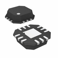
ADCMP605BCPZ-WP Analog Devices Inc, ADCMP605BCPZ-WP Datasheet - Page 10

ADCMP605BCPZ-WP
Manufacturer Part Number
ADCMP605BCPZ-WP
Description
IC,VOLT COMPARATOR,SINGLE,LLCC,12PIN,PLASTIC
Manufacturer
Analog Devices Inc
Type
with Latchr
Datasheet
1.ADCMP604BKSZ-REEL7.pdf
(16 pages)
Specifications of ADCMP605BCPZ-WP
Number Of Elements
1
Output Type
Complementary, LVDS, Rail-to-Rail
Voltage - Supply
2.5 V ~ 5.5 V, ±1.25 V ~ 2.75 V
Mounting Type
Surface Mount
Package / Case
12-VFQFN, CSP Exposed Pad
No. Of Comparators
1
Ic Output Type
LVDS
Supply Current
1.6mA
Supply Voltage Range
2.5V To 5.5V
Amplifier Case Style
LFCSP
No. Of Pins
12
Operating Temperature Range
-40°C To +125°C
Lead Free Status / RoHS Status
Lead free / RoHS Compliant
Available stocks
Company
Part Number
Manufacturer
Quantity
Price
Company:
Part Number:
ADCMP605BCPZ-WP
Manufacturer:
SANYO
Quantity:
12 000
Part Number:
ADCMP605BCPZ-WP
Manufacturer:
ADI/亚德诺
Quantity:
20 000
ADCMP604/ADCMP605
APPLICATION INFORMATION
POWER/GROUND LAYOUT AND BYPASSING
The ADCMP604/ADCMP605 comparators are very high speed
devices. Despite the low noise output stage, it is essential to use
proper high speed design techniques to achieve the specified
performance. Because comparators are uncompensated amplifiers,
feedback in any phase relationship is likely to cause oscillations
or undesired hysteresis. The use of low impedance supply
planes is of critical importance particularly the output supply
plane (V
planes are recommended as part of a multilayer board.
Providing the lowest inductance return path for switching
currents ensures the best possible performance in the target
application.
It is also important to adequately bypass the input and output
supplies. Multiple high quality 0.01 μF bypass capacitors should
be placed as close as possible to each of the V
pins and should be connected to the GND plane with redundant
vias. At least one of these should be placed to provide a physically
short return path for output currents flowing back from ground
to the V
should be carefully selected for minimum inductance and ESR.
Parasitic layout inductance should also be strictly controlled to
maximize the effectiveness of the bypass at high frequencies.
If the package allows, and the input and output supplies have
been connected separately (V
of these supplies separately to the GND plane. Do not connect a
bypass capacitor between these supplies. It is recommended that
the GND plane separate the V
circuit board layout is designed to minimize coupling between
the two supplies to take advantage of the additional bypass
capacitance from each respective supply to the ground plane.
This enhances the performance when split input/output supplies
are used. If the input and output supplies are connected together
for single-supply operation (V
two supplies is unavoidable; however, careful board placement
can help keep output return currents away from the inputs.
CCI
CCO
pin and the V
) and the ground plane (GND). Individual supply
CCO
pin. High frequency bypass capacitors
CCI
CCI
CCI
≠ V
and V
= V
CCO
CCO
CCO
), be sure to bypass each
), coupling between the
planes when the
CCI
and V
CCO
supply
Rev. A | Page 10 of 16
LVDS-COMPATIBLE OUTPUT STAGE
Specified propagation delay dispersion performance is only
achieved by keeping parasitic capacitive loads at or below the
specified minimums. The outputs of the ADCMP604 and
ADCMP605 are designed to directly drive any standard LVDS-
compatible input.
USING/DISABLING THE LATCH FEATURE
The latch input is designed for maximum versatility. It can
safely be left floating or it can be driven low by any standard
TTL/CMOS device as a high speed latch. In addition, the pin
can be operated as a hysteresis control pin with a bias voltage of
1.25 V nominal and an input resistance of approximately
70 kΩ. This allows the comparator hysteresis to be easily
controlled by either a resistor or an inexpensive CMOS DAC.
Driving this pin high or floating the pin disables all hysteresis.
Hysteresis control and latch mode can be used together if an
open drain, an open collector, or a three-state driver is connected in
parallel to the hysteresis control resistor or current source.
Due to the programmable hysteresis feature, the logic threshold
of the latch pin is approximately 1.1 V, regardless of V
OPTIMIZING PERFORMANCE
As with any high speed comparator, proper design and layout
techniques are essential for obtaining the specified performance.
Stray capacitance, inductance, inductive power and ground
impedances, or other layout issues can severely limit performance
and often cause oscillation. Large discontinuities along input
and output transmission lines can also limit the specified pulse-
width dispersion performance. The source impedance should
be minimized as much as is practicable. High source impedance,
in combination with the parasitic input capacitance of the
comparator, causes an undesirable degradation in bandwidth at
the input, thus degrading the overall response. Thermal noise
from large resistances can easily cause extra jitter with slowly
slewing input signals. Higher impedances encourage undesired
coupling.
CCO
.


