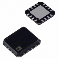
ADP1653ACPZ-R7 Analog Devices Inc, ADP1653ACPZ-R7 Datasheet - Page 7

ADP1653ACPZ-R7
Manufacturer Part Number
ADP1653ACPZ-R7
Description
IC,Laser Diode/LED Driver,LLCC,16PIN,PLASTIC
Manufacturer
Analog Devices Inc
Type
Photo Flash LEDr
Datasheet
1.ADP1653ACPZ-R7.pdf
(24 pages)
Specifications of ADP1653ACPZ-R7
Topology
PWM, Step-Up (Boost)
Number Of Outputs
1
Internal Driver
Yes
Type - Primary
Flash/Torch
Frequency
1.2MHz
Voltage - Supply
3 V ~ 5.5 V
Mounting Type
Surface Mount
Package / Case
16-LFCSP
Operating Temperature
-40°C ~ 125°C
Current - Output / Channel
200mA, 500mA
Internal Switch(s)
Yes
Efficiency
92%
Lead Free Status / RoHS Status
Lead free / RoHS Compliant
Voltage - Output
-
Lead Free Status / RoHS Status
Lead free / RoHS Compliant
Other names
ADP1653ACPZ-R7TR
Available stocks
Company
Part Number
Manufacturer
Quantity
Price
Company:
Part Number:
ADP1653ACPZ-R7
Manufacturer:
AD
Quantity:
27 356
PIN CONFIGURATION AND FUNCTION DESCRIPTIONS
Table 5. Pin Function Descriptions
Pin No.
1
2
3
4
5
6
7
8
9
10
11
12
13
14
15
16
Mnemonic
SETT
SETF
CTRL1/SCL
CTRL0/SDA
SETI
ILED
OUT
GND
HPLED
INTF
INT
PGND
LX
V
EN
STR
DD
Description
Set Torch Input (2-Bit Logic Interface Only). SETT programs the high power LED current in torch mode. An
external resistor connected between SETT and ground sets the torch current. When SETT is tied high, the current
is internally set to 125 mA. In I
Set Flash Input. SETF programs the high power LED (HPLED) current in flash mode and allows for transmit
blanking of the LED. In 2-bit logic interface mode, an external resistor connected between SETF and ground sets
the flash current. If SETF is tied high, the current is set internally to 500 mA. In I
with both the external resistor and the internal HPLED bits in the output select register. If SETF is tied high, an
internal 50 kΩ resistor combined with the HPLED bits set the HPLED current.
Serial Interface Clock Input. In 2-bit logic interface mode, CTRL1 is the second input bit of the digital interface.
In I
Serial Interface Data Input. In 2-bit logic interface mode, CTRL0 is the first input bit of the digital interface.
In I
Set Indicator Input (2-Bit Logic Interface Only). SETI programs the indicator LED current. An external resistor connected
between SETI and ground sets the indicator LED (ILED) current. If SETI is tied high, the current is internally set to
10 mA. In I
Indicator LED Input. Connect the cathode of the indicator LED to the ILED pin. Connect the anode to the battery
or to a voltage rail greater than the LED forward voltage.
White LED Output Voltage. OUT senses the output voltage of the white LED step-up converter. At startup, the
ADP1653 limits the rate of increase of the voltage at OUT (soft start) to prevent excessive input inrush current.
The OUT pin features a comparator to detect an overvoltage condition if the LED string is open circuited. Connect
the anode of the white LED(s) to OUT. Connect a 3.3 μF or greater capacitor between OUT and PGND.
Analog/Digital Ground. Connect GND to PGND at the LFCSP paddle.
High Power LED Current Regulator. HPLED regulates the current of the high power LED(s). Connect the cathode of
the white LED string to HPLED.
Interface Input. INTF selects the 2-pin interface mode. INTF is driven high to enable CTRL1 and CTRL0 for 2-bit
logic interface mode. INTF is driven low to enable SDA and SCL for I
Active Low Interrupt Output. INT is an open-drain output that transitions from high to low to signal that a fault
condition has occurred. INT should be connected via a pull-up resistor (for example, 10 kΩ to 100 kΩ) to the I/O
supply rail and directly to the system processor. When an interrupt is detected, the system processor can read the
FAULT register, using the I
Power Ground for Internal Switching FET.
White LED Switch Node. LX drives the inductor of the white LED step-up converter. An inductor and diode
connected to LX powers the white LEDs.
Supply Input. Connect the battery between V
Enable Input. CMOS input. Driving EN high turns on the ADP1653. Driving EN low disables the ADP1653 and
reduces the input current to less than 1 μA. When EN is high, disabling the LEDs puts the part into sleep mode,
dropping the input current to less than 45 μA.
Strobe Control Input (I
LED. STR also enables the watchdog timer to prevent overstressing the white LEDs.
2
2
C mode, SCL is the clock input of the I
C mode, SDA is the data input/output of the I
2
C mode, this pin is regarded as a no connect.
2
C Interface Only). CMOS input. Driving STR high enables the flash function of the white
CTRL0/SDA
CTRL1/SCL
2
C interface for details on the fault condition.
SETT
SETF
2
C mode, this pin is regarded as a no connect.
Figure 4. Pin Configuration
1
2
3
4
Rev. B | Page 7 of 24
(Not to Scale)
ADP1653
TOP VIEW
PIN 1
INDICATOR
2
C-compatible serial interface.
DD
and PGND. Bypass V
2
C-compatible serial interface.
12 PGND
11 INT
10 INTF
9 HPLED
DD
2
to PGND with a 4.7 μF or greater capacitor.
C interfacing.
2
C mode, the flash current scales
ADP1653


