ADSP-21261SKBC-150 Analog Devices Inc, ADSP-21261SKBC-150 Datasheet - Page 18
ADSP-21261SKBC-150
Manufacturer Part Number
ADSP-21261SKBC-150
Description
150 MHz, 32Bit DSP Processor.
Manufacturer
Analog Devices Inc
Series
SHARC®r
Type
Fixed/Floating Pointr
Datasheet
1.ADSP-21261SKBCZ150.pdf
(44 pages)
Specifications of ADSP-21261SKBC-150
Interface
DAI, SPI
Clock Rate
150MHz
Non-volatile Memory
ROM (384 kB)
On-chip Ram
128kB
Voltage - I/o
3.30V
Voltage - Core
1.20V
Operating Temperature
0°C ~ 70°C
Mounting Type
Surface Mount
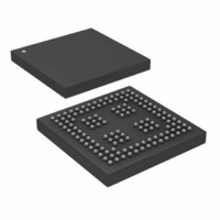
Package / Case
136-CSPBGA
Lead Free Status / RoHS Status
Contains lead / RoHS non-compliant
Available stocks
Company
Part Number
Manufacturer
Quantity
Price
Company:

Part Number:
ADSP-21261SKBC-150
Manufacturer:
AD
Quantity:
30


ADSP-21261
Power-Up Sequencing
The timing requirements for DSP startup are given in
and
Table 9. Power-Up Sequencing (DSP Startup)
1
2
3
4
5
Parameter
Timing Requirements
t
t
t
t
t
Switching Characteristic
t
Valid V
Assumes a stable CLKIN signal, after meeting worst-case startup timing of crystal oscillators. Refer to the crystal oscillator manufacturer’s data sheet for startup time. Assume
Based on CLKIN cycles.
Applies after the power-up sequence is complete. Subsequent resets require a minimum of four CLKIN cycles for RESET to be held low in order to properly initialize and
The 4096 cycle count depends on t
RSTVDD
IVDDEVDD
CLKVDD
CLKRST
PLLRST
CORERST
depending on the design of the power supply subsystem.
a 25 ms maximum oscillator startup time if using the XTAL pin and internal oscillator circuit in conjunction with an external crystal.
propagate default states at all I/O pins.
cycles maximum.
Figure
DDINT
/V
6.
DDEXT
assumes that the supplies are fully ramped to their 1.2 and 3.3 volt rails. Voltage ramp rates can vary from microseconds to hundreds of milliseconds
CLKCFG1–0
V DDEXT
RSTOUT
RESET Low Before V
V
CLKIN Valid After V
CLKIN Valid Before RESET Deasserted
PLL Control Setup Before RESET Deasserted
DSP Core Reset Deasserted After RESET Deasserted
V DDINT
RESET
DDINT
CLKIN
SRST
On Before V
*
*
specification in
MULTIPLEXED WITH CLKOUT
t
RSTVDD
DDEXT
DDINT
DDINT
Table
/V
/V
DDEXT
DDEXT
11. If setup time is not met, one additional CLKIN cycle may be added to the core reset time, resulting in 4097
Rev. 0 | Page 18 of 44 | March 2006
Valid
Figure 6. Power-Up Sequencing
On
Table 9
1
t
IVDDEVDD
t
PLLRST
t
t
CLKVDD
CLKRST
Min
0
–50
0
10
20
4096t
t
CORERST
2
3
CK
4, 5
Max
+200
200
Unit
ns
ms
ms
μs
μs
Related parts for ADSP-21261SKBC-150
Image
Part Number
Description
Manufacturer
Datasheet
Request
R

Part Number:
Description:
±1.7g Dual-Axis IMEMS Accelerometer Evaluation Board
Manufacturer:
Analog Devices Inc
Datasheet:

Part Number:
Description:
Inertial Sensor Evaluation System
Manufacturer:
Analog Devices Inc
Datasheet:
Part Number:
Description:
Manufacturer:
Analog Devices Inc
Datasheet:
Part Number:
Description:
Manufacturer:
Analog Devices Inc
Datasheet:
Part Number:
Description:
Manufacturer:
Analog Devices Inc
Datasheet:
Part Number:
Description:
Manufacturer:
Analog Devices Inc
Datasheet:
Part Number:
Description:
Manufacturer:
Analog Devices Inc
Datasheet:
Part Number:
Description:
Manufacturer:
Analog Devices Inc
Datasheet:
Part Number:
Description:
Manufacturer:
Analog Devices Inc
Datasheet:
Part Number:
Description:
Manufacturer:
Analog Devices Inc
Datasheet:
Part Number:
Description:
Manufacturer:
Analog Devices Inc
Datasheet:
Part Number:
Description:
Manufacturer:
Analog Devices Inc
Datasheet:
Part Number:
Description:
Manufacturer:
Analog Devices Inc
Datasheet: