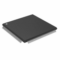
ADSP-2191MBSTZ-140 Analog Devices Inc, ADSP-2191MBSTZ-140 Datasheet - Page 34

ADSP-2191MBSTZ-140
Manufacturer Part Number
ADSP-2191MBSTZ-140
Description
IC,DSP,16-BIT,CMOS,QFP,144PIN,PLASTIC
Manufacturer
Analog Devices Inc
Series
ADSP-21xxr
Type
Fixed Pointr
Specifications of ADSP-2191MBSTZ-140
Interface
Host Interface, SPI, SSP, UART
Clock Rate
140MHz
Non-volatile Memory
External
On-chip Ram
160kB
Voltage - I/o
3.00V, 3.30V
Voltage - Core
2.50V
Operating Temperature
-40°C ~ 85°C
Mounting Type
Surface Mount
Package / Case
144-LQFP
Device Core Size
16b
Clock Freq (max)
140MHz
Mips
140
Device Input Clock Speed
140MHz
Ram Size
160KB
Operating Supply Voltage (typ)
2.5/3.3V
Operating Supply Voltage (min)
2.37/2.97V
Operating Supply Voltage (max)
2.63/3.6V
Operating Temp Range
-40C to 85C
Operating Temperature Classification
Industrial
Mounting
Surface Mount
Pin Count
144
Package Type
LQFP
Lead Free Status / RoHS Status
Lead free / RoHS Compliant
Lead Free Status / RoHS Status
Lead free / RoHS Compliant
Other names
ADSP-2191MBSTZ140
Available stocks
Company
Part Number
Manufacturer
Quantity
Price
Company:
Part Number:
ADSP-2191MBSTZ-140
Manufacturer:
MAXIM
Quantity:
101
Company:
Part Number:
ADSP-2191MBSTZ-140
Manufacturer:
Analog Devices Inc
Quantity:
10 000
ADSP-2191M
Serial Ports
Table 19
Sync operations.
Table 19. Serial Ports
1
2
3
4
5
6
7
To determine whether communication is possible between two devices at clock speed n, the following specifications must be confirmed: 1) frame sync delay
Word selected timing for I
Referenced to sample edge.
Referenced to drive edge.
Only applies to SPORT0/1.
MCE=1, TFS enable, and TFS valid follow t
If external RFSD/TFS setup to RCLK/TCLK>0.5t
Parameter
External Clock
Timing Requirements
t
t
t
t
t
t
Internal Clock
Timing Requirements
t
t
t
t
External or Internal Clock
Switching Characteristics
t
t
External Clock
Switching Characteristics
t
t
Internal Clock
Switching Characteristics
t
t
t
Enable and Three-State
Switching Characteristics
t
t
t
t
External Late Frame Sync
Switching Characteristics
t
t
and frame sync setup-and-hold, 2) data delay and data setup-and-hold, and 3) SCLK width.
SFSE
HFSE
SDRE
HDRE
SCLKW
SCLK
SFSI
HFSI
SDRI
HDRI
DFSE
HOFSE
DDTE
HDTE
DDTI
HDTI
SCLKIW
DTENE
DDTTE
DTENI
DDTTI
DDTLFSE
DTENLFSE
and
Figure 18
TFS/RFS Setup Before TCLK/RCLK
TFS/RFS Hold After TCLK/RCLK
Receive Data Setup Before RCLK
Receive Data Hold After RCLK
TCLK/RCLK Width
TCLK/RCLK Period
TFS Setup Before TCLK
TFS/RFS Hold After TCLK/RCLK
Receive Data Setup Before RCLK
Receive Data Hold After RCLK
TFS/RFS Delay After TCLK/RCLK (Internally
Generated FS)
TFS/RFS Hold After TCLK/RCLK (Internally
Generated FS)
Transmit Data Delay After TCLK
Transmit Data Hold After TCLK
Transmit Data Delay After TCLK
Transmit Data Hold After TCLK
TCLK/RCLK Width
Data Enable from External TCLK
Data Disable from External TCLK
Data Enable from Internal TCLK
Data Disable from External TCLK
Data Delay from Late External TFS with MCE=1, MFD=0
Data Enable from Late FS or MCE=1, MFD=0
2
describe SPORT transmit and receive operations, while
S mode is the same as TFS/RFS timing (normal framing only).
1, 2
5
4
4
DDTENFS
4
LSCK
; RFS Setup Before RCLK
and t
, t
DDTLSCK
3
3
DDTLFSE
4
4
4
3
3
4
4
4
4
4
3
3
3
and t
.
–34–
DTENLSCK
6, 7
apply; otherwise t
3
Figure 19
6, 7
Min
4
4
1.5
4
0.5t
2t
4
3
2
5
3
4
4
0.5t
0
0
3.5
HCLK
DDTLFSE
and
HCLK
HCLK
Figure 20
–1
–3.5
and t
DTENLFS
describe SPORT Frame
Max
14
13.4
13.4
0.5t
12.1
13
13
12
10.5
HCLK
apply.
+2.5
REV. 0
Unit
ns
ns
ns
ns
ns
ns
ns
ns
ns
ns
ns
ns
ns
ns
ns
ns
ns
ns
ns
ns
ns
ns
ns


