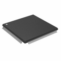
ADSP-2191MBSTZ-140 Analog Devices Inc, ADSP-2191MBSTZ-140 Datasheet - Page 6

ADSP-2191MBSTZ-140
Manufacturer Part Number
ADSP-2191MBSTZ-140
Description
IC,DSP,16-BIT,CMOS,QFP,144PIN,PLASTIC
Manufacturer
Analog Devices Inc
Series
ADSP-21xxr
Type
Fixed Pointr
Specifications of ADSP-2191MBSTZ-140
Interface
Host Interface, SPI, SSP, UART
Clock Rate
140MHz
Non-volatile Memory
External
On-chip Ram
160kB
Voltage - I/o
3.00V, 3.30V
Voltage - Core
2.50V
Operating Temperature
-40°C ~ 85°C
Mounting Type
Surface Mount
Package / Case
144-LQFP
Device Core Size
16b
Clock Freq (max)
140MHz
Mips
140
Device Input Clock Speed
140MHz
Ram Size
160KB
Operating Supply Voltage (typ)
2.5/3.3V
Operating Supply Voltage (min)
2.37/2.97V
Operating Supply Voltage (max)
2.63/3.6V
Operating Temp Range
-40C to 85C
Operating Temperature Classification
Industrial
Mounting
Surface Mount
Pin Count
144
Package Type
LQFP
Lead Free Status / RoHS Status
Lead free / RoHS Compliant
Lead Free Status / RoHS Status
Lead free / RoHS Compliant
Other names
ADSP-2191MBSTZ140
Available stocks
Company
Part Number
Manufacturer
Quantity
Price
Company:
Part Number:
ADSP-2191MBSTZ-140
Manufacturer:
MAXIM
Quantity:
101
Company:
Part Number:
ADSP-2191MBSTZ-140
Manufacturer:
Analog Devices Inc
Quantity:
10 000
ADSP-2191M
different mechanisms to generate a 24-bit address for each bus.
The DSP has three functions that support access to the full
memory map.
The ADSP-2191M has 1K word of on-chip ROM that holds boot
routines. If peripheral booting is selected, the DSP starts
executing instructions from the on-chip boot ROM, which starts
the boot process from the selected peripheral.
tion, see “Booting Modes” on page 11.
is located on Page 255 in the DSP’s memory space map.
External (Off-Chip) Memory
Each of the ADSP-2191M’s off-chip memory spaces has a
separate control register, so applications can configure unique
access parameters for each space. The access parameters include
read and write wait counts, waitstate completion mode, I/O clock
divide ratio, write hold time extension, strobe polarity, and data
bus width. The core clock and peripheral clock ratios influence
the external memory access strobe widths.
see “Clock Signals” on page 11.
All of these off-chip memory spaces are accessible through the
External Port, which can be configured for data widths of
8 or 16 bits.
The DAGs generate 24-bit addresses for data fetches from
the entire DSP memory address range. Because DAG
index (address) registers are 16 bits wide and hold the
lower 16 bits of the address, each of the DAGs has its own
8-bit page register (DMPGx) to hold the most significant
eight address bits. Before a DAG generates an address,
the program must set the DAG’s DMPGx register to the
appropriate memory page.
The Program Sequencer generates the addresses for
instruction fetches. For relative addressing instructions,
the program sequencer bases addresses for relative jumps,
calls, and loops on the 24-bit Program Counter (PC). In
direct addressing instructions (two-word instructions),
the instruction provides an immediate 24-bit address
value. The PC allows linear addressing of the full 24-bit
address range.
For indirect jumps and calls that use a 16-bit DAG
address register for part of the branch address, the
Program Sequencer relies on an 8-bit Indirect Jump page
(IJPG) register to supply the most significant eight
address bits. Before a cross page jump or call, the program
must set the program sequencer’s IJPG register to the
appropriate memory page.
External memory space (MS3–0 pins)
I/O memory space (IOMS pin)
Boot memory space (BMS pin)
The off-chip memory spaces are:
The on-chip boot ROM
For more information,
For more informa-
–6–
External Memory Space
External memory space consists of four memory banks. These
banks can contain a configurable number of 64K word pages. At
reset, the page boundaries for external memory have Bank0
containing pages 1 63, Bank1 containing pages 64 127, Bank2
containing pages 128 191, and Bank3 that contains pages
192 254. The MS3–0 memory bank pins select Banks 3–0,
respectively. The external memory interface is byte-addressable
and decodes the 8 MSBs of the DSP program address to select
one of the four banks. Both the ADSP-219x core and DMA-capa-
ble peripherals can access the DSP’s external memory space.
I/O Memory Space
The ADSP-2191M supports an additional external memory
called I/O memory space. This space is designed to support
simple connections to peripherals (such as data converters and
external registers) or to bus interface ASIC data registers. I/O
space supports a total of 256K locations. The first 8K addresses
are reserved for on-chip peripherals. The upper 248K addresses
are available for external peripheral devices. The DSP’s instruc-
tion set provides instructions for accessing I/O space. These
instructions use an 18-bit address that is assembled from an
8-bit I/O page (IOPG) register and a 10-bit immediate value
supplied in the instruction. Both the ADSP-219x core and a Host
(through the Host Port Interface) can access I/O memory space.
Boot Memory Space
Boot memory space consists of one off-chip bank with 63 pages.
The BMS memory bank pin selects boot memory space. Both
the ADSP-219x core and DMA-capable peripherals can access
the DSP’s off-chip boot memory space. After reset, the DSP
always starts executing instructions from the on-chip boot ROM.
Depending on the boot configuration, the boot ROM code can
start booting the DSP from boot memory.
see “Booting Modes” on page 11.
Interrupts
The interrupt controller lets the DSP respond to 17 interrupts
with minimum overhead. The controller implements an interrupt
priority scheme as shown in
unassigned slots for software and peripheral interrupts.
Table 2
eral interrupts. To assign the peripheral interrupts a different
priority, applications write the new priority to their correspond-
ing control bits (determined by their ID) in the Interrupt Priority
Control register. The peripheral interrupt’s position in the
IMASK and IRPTL register and its vector address depend on its
priority level, as shown in
IRPTL registers are limited to 16 bits, any peripheral interrupts
shows the ID and priority at reset of each of the periph-
Table
Table
1. Because the IMASK and
1. Applications can use the
For more information,
REV. 0


