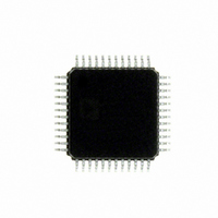
ADUC7060BSTZ32 Analog Devices Inc, ADUC7060BSTZ32 Datasheet - Page 92

ADUC7060BSTZ32
Manufacturer Part Number
ADUC7060BSTZ32
Description
DUAL 24-BIT AFE AND ARM 7 I.C
Manufacturer
Analog Devices Inc
Series
MicroConverter® ADuC7xxxr
Specifications of ADUC7060BSTZ32
Design Resources
4 mA-to-20 mA Loop-Powered Temperature Monitor Using ADuC7060/1 (CN0145) Low power, Long Range, ISM Wireless Measuring Node (CN0164)
Core Processor
ARM7
Core Size
16/32-Bit
Speed
10MHz
Connectivity
I²C, SPI, UART/USART
Peripherals
POR, PWM, Temp Sensor, WDT
Number Of I /o
14
Program Memory Size
32KB (16K x 16)
Program Memory Type
FLASH
Ram Size
4K x 8
Voltage - Supply (vcc/vdd)
2.375 V ~ 2.625 V
Data Converters
A/D 5x24b, 8x24b, D/A 1x14b
Oscillator Type
Internal
Operating Temperature
-40°C ~ 125°C
Package / Case
48-LQFP
Cpu Family
ADuC7xxx
Device Core
ARM7TDMI
Device Core Size
16/32Bit
Frequency (max)
10.24MHz
Interface Type
I2C/SPI/UART
Total Internal Ram Size
4KB
# I/os (max)
14
Number Of Timers - General Purpose
4
Operating Supply Voltage (typ)
2.5V
Operating Supply Voltage (max)
2.625V
Operating Supply Voltage (min)
2.375V
On-chip Adc
2(4-chx24-bit)
Instruction Set Architecture
RISC
Operating Temp Range
-40C to 125C
Operating Temperature Classification
Automotive
Mounting
Surface Mount
Pin Count
48
Package Type
LQFP
Package
48LQFP
Family Name
ADuC7xxx
Maximum Speed
10.24 MHz
Operating Supply Voltage
2.5 V
Data Bus Width
16|32 Bit
Number Of Programmable I/os
14
Number Of Timers
4
Lead Free Status / RoHS Status
Lead free / RoHS Compliant
Eeprom Size
-
Lead Free Status / Rohs Status
Compliant
Available stocks
Company
Part Number
Manufacturer
Quantity
Price
Company:
Part Number:
ADUC7060BSTZ32
Manufacturer:
CYPRESS
Quantity:
294
Company:
Part Number:
ADUC7060BSTZ32
Manufacturer:
ADI
Quantity:
315
Company:
Part Number:
ADUC7060BSTZ32
Manufacturer:
Analog Devices Inc
Quantity:
10 000
Part Number:
ADUC7060BSTZ32
Manufacturer:
ADI/亚德诺
Quantity:
20 000
Company:
Part Number:
ADUC7060BSTZ32-RL
Manufacturer:
Analog Devices Inc
Quantity:
10 000
ADuC7060/ADuC7061
I
Name:
Address:
Default value:
Access:
Function:
Table 104. I2CSSTA MMR Bit Designations
Bit
15
14
13
12:11
10
9:8
7
6
5
4
3
2
C Slave Status, I2CSSTA, Register
Name
I2CSTA
I2CREPS
I2CID[1:0]
I2CSS
I2CGCID[1:0]
I2CGC
I2CSBUSY
I2CSNA
I2CSRxFO
I2CSRXQ
I2CSSTA
0xFFFF092C
0x0000
Read and write
This 16-bit MMR is the I
Description
Reserved bit.
This bit is set to 1 if a start condition followed by a matching address is detected, a start byte (0x01) is received, or
general calls are enabled and a general call code of 0x00 is received.
This bit is cleared on receiving a stop condition
This bit is set to 1 if a repeated start condition is detected.
This bit is cleared on receiving a stop condition.
I
[00] = received address matches I2CID0.
[01] = received address matches I2CID1.
[10] = received address matches I2CID2.
[11] = received address matches I2CID3.
I
This bit is set to 1 when a stop condition is detected after a previous start and matching address. When the
I2CSSENI bit in I2CSCON is set, an interrupt is generated.
This bit is cleared by reading this register.
I
[00] = no general call received.
[01] = general call reset and program address.
[10] = general program address.
[11] = general call matching alternative ID.
Note that these bits are not cleared by a general call reset command.
Clear these bits by writing a 1 to the I2CGCCLR bit in I2CSCON.
I
This bit is set to 1 if the slave receives a general call command of any type. If the command received was a reset
command, then all registers return to their default states. If the command received was a hardware general call,
the receive FIFO holds the second byte of the command, and this can be compared with the I2CALT register.
Clear this bit by writing a 1 to the I2CGCCLR bit in I2CSCON.
I
Set to 1 when the slave receives a start condition.
Cleared by hardware if the received address does not match any of the I2CIDx registers, the slave device receives
a stop condition, or a repeated start address does not match any of the I2CIDx registers.
I
This bit is set to 1 when the slave responds to a bus address with a no acknowledge. This bit is asserted under the
following conditions: if a no acknowledge was returned because there was no data in the transmit FIFO or if the
I2CNACKEN bit was set in the I2CSCON register.
This bit is cleared in all other conditions.
Slave receive FIFO overflow.
This bit is set to 1 when a byte is written to the receive FIFO when it is already full.
This bit is cleared in all other conditions.
I
This bit is set to 1 when the receive FIFO of the slave is not empty. This bit causes an interrupt to occur if the
I2CSRXENI bit in I2CSCON is set.
The receive FIFO must be read or flushed to clear this bit.
2
2
2
2
2
2
2
C address matching register. These bits indicate which I2CIDx register matches the received address.
C stop condition after start detected bit.
C general call ID bits.
C general call status bit.
C slave busy status bit.
C slave no acknowledge data bit.
C slave receive request bit.
2
C status register in slave mode.
Rev. B | Page 92 of 108


