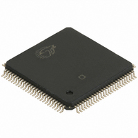
CY7C028V-15AXC Cypress Semiconductor Corp, CY7C028V-15AXC Datasheet - Page 7

CY7C028V-15AXC
Manufacturer Part Number
CY7C028V-15AXC
Description
IC,SRAM,64KX16,CMOS,QFP,100PIN,PLASTIC
Manufacturer
Cypress Semiconductor Corp
Datasheet
1.CY7C027V-15AXC.pdf
(22 pages)
Specifications of CY7C028V-15AXC
Format - Memory
RAM
Memory Type
SRAM - Dual Port, Asynchronous
Memory Size
1M (64K x 16)
Speed
15ns
Interface
Parallel
Voltage - Supply
3 V ~ 3.6 V
Operating Temperature
0°C ~ 70°C
Package / Case
100-LQFP
Lead Free Status / RoHS Status
Lead free / RoHS Compliant
Other names
428-1755
CY7C028V-15AXC
CY7C028V-15AXC
Available stocks
Company
Part Number
Manufacturer
Quantity
Price
Company:
Part Number:
CY7C028V-15AXC
Manufacturer:
Cypress Semiconductor Corp
Quantity:
10 000
Company:
Part Number:
CY7C028V-15AXCT
Manufacturer:
Cypress Semiconductor Corp
Quantity:
10 000
Maximum Ratings
Exceeding maximum ratings may shorten the useful life of the
device. User guidelines are not tested.
Storage temperature ................................ –65
Ambient temperature with
power applied ........................................... –55
Supply voltage to ground potential ...............–0.5 V to +4.6 V
DC voltage applied to
outputs in High-Z state........................... –0.5 V to V
Electrical Characteristics
Capacitance
Document #: 38-06078 Rev. *D
V
V
V
V
I
I
I
I
I
I
I
C
C
Notes
Parameter
IX
OZ
CC
SB1
SB2
SB3
SB4
8. Pulse width < 20 ns.
9. Industrial parts are available in CY7C028V and CY7C038V, CY7C027V/027AV only.
10. f
11. Tested initially and after any design or process changes that may affect these parameters.
OH
OL
IH
IL
IN
OUT
MAX
= 1/t
Parameter
RC
Output HIGH voltage
(V
Output LOW voltage (V
Input HIGH voltage
Input LOW voltage
Input leakage current
Output leakage current
Operating current (V
mA) outputs disabled
Standby current (Both ports TTL
level) CE
Standby current (One port TTL level)
CE
Standby current (Both ports CMOS
level) CE
Standby current (One port CMOS
level) CE
= All inputs cycling at f = 1/t
CC
L
| CE
=Min., I
[11]
L
R
L
L
& CE
& CE
| CE
V
OH
IH
Input capacitance
Output capacitance
= –4.0 mA)
R
R
R
, f=f
V
Description
V
V
RC
MAX
CC
IH
IH
CC
(except output enable). f = 0 means no address or control lines change. This applies only to inputs at CMOS level standby I
, f=f
CC
=Max. I
, f=f
Description
0.2 V, f=0
Over the Operating Range
=Min., I
MAX
MAX
[10]
OUT
OH
C to +150
C to +125
=0
= +4.0 mA)
CC
Com’l.
Com’l.
Com’l.
Com’l.
Com’l.
Ind.
Ind.
Ind.
Ind.
Ind.
+0.5 V
[9]
[9]
[9]
[9]
[9]
T
V
C
C
A
CC
= 25
Min
–10
2.4
2.2
= 3.3 V
5
–
–
Test Conditions
C, f = 1 MHz,
CY7C027V/027AV/028V/CY7C037AV/CY7C038V
DC input voltage
Output current into outputs (LOW) .............................. 20 mA
Static discharge voltage.......................................... > 1100 V
Latch-up current .................................................... > 200 mA
Operating Range
Commercial
Industrial
-15
Typ
125
35
80
10
75
–
–
–
–
–
–
Range
Max
250
185
120
105
0.4
0.8
10
50
–
5
[9]
Min
–10
2.4
2.2
5
–
–
–
[8]
................................. –0.5 V to V
Typ
120
140
-20
10
35
45
75
85
10
70
80
–
–40
0
Temperature
CY7C027V/027AV/028V
Ambient
C to +70
Max
C to +85
175
195
110
120
250
250
105
0.4
0.8
10
45
55
95
–
–
5
Max
10
10
CY7C037AV/038V
Min
–10
2.4
2.2
5
–
–
–
C
C
Typ
115
-25
30
65
10
60
–
3.3 V 300 mV
3.3 V 300 mV
–
–
–
–
–
Max
165
250
0.4
0.8
10
40
95
80
Page 7 of 22
Unit
–
–
5
CC
V
pF
pF
SB3
CC
+0.5 V
.
Unit
mA
mA
mA
mA
mA
mA
mA
mA
A
A
A
A
V
V
V
V
[+] Feedback


