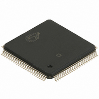
CY7C028V-15AXC Cypress Semiconductor Corp, CY7C028V-15AXC Datasheet - Page 8

CY7C028V-15AXC
Manufacturer Part Number
CY7C028V-15AXC
Description
IC,SRAM,64KX16,CMOS,QFP,100PIN,PLASTIC
Manufacturer
Cypress Semiconductor Corp
Datasheet
1.CY7C027V-15AXC.pdf
(22 pages)
Specifications of CY7C028V-15AXC
Format - Memory
RAM
Memory Type
SRAM - Dual Port, Asynchronous
Memory Size
1M (64K x 16)
Speed
15ns
Interface
Parallel
Voltage - Supply
3 V ~ 3.6 V
Operating Temperature
0°C ~ 70°C
Package / Case
100-LQFP
Lead Free Status / RoHS Status
Lead free / RoHS Compliant
Other names
428-1755
CY7C028V-15AXC
CY7C028V-15AXC
Available stocks
Company
Part Number
Manufacturer
Quantity
Price
Company:
Part Number:
CY7C028V-15AXC
Manufacturer:
Cypress Semiconductor Corp
Quantity:
10 000
Company:
Part Number:
CY7C028V-15AXCT
Manufacturer:
Cypress Semiconductor Corp
Quantity:
10 000
Switching Characteristics
Document #: 38-06078 Rev. *D
OUTPUT
t
t
t
t
t
t
t
t
t
t
t
t
t
t
t
t
t
t
t
Notes
RC
AA
OHA
ACE
DOE
LZOE
HZOE
LZCE
HZCE
PU
PD
ABE
WC
SCE
AW
HA
SA
PWE
SD
12. Test conditions assume signal transition time of 3 ns or less, timing reference levels of 1.5 V, input pulse levels of 0 to 3.0 V, and output loading of the specified
13. To access RAM, CE=L, UB=L, SEM=H. To access semaphore, CE=H and SEM=L. Either condition must be valid for the entire t
14. At any given temperature and voltage condition for any given device, t
15. Test conditions used are Load 2.
16. This parameter is guaranteed by design, but it is not production tested. For information on port-to-port delay through RAM cells from writing port to reading port,
Read Cycle
Write Cycle
C = 30 pF
Parameter
(a) Normal Load (Load 1)
[16]
[16]
[13]
I
refer to
[13]
[13]
[13]
OI
[14, 15, 16]
[14, 15, 16]
[14, 15, 16]
[14, 15, 16]
/I
OH
and 30 pF load capacitance.
Figure
11.
Read cycle time
Address to data valid
Output hold from address change
CE LOW to data valid
OE LOW to data valid
OE LOW to Low Z
OE HIGH to High Z
CE LOW to Low Z
CE HIGH to High Z
CE LOW to power-up
CE HIGH to power-down
Byte enable access time
Write cycle time
CE LOW to write end
Address valid to write end
Address hold from write end
Address setup to write start
Write pulse width
Data setup to write end
3.3 V
R1 = 590
R2 = 435
Description
Over the Operating Range
GND
3.0V
Figure 3. AC Test Loads and Waveforms
OUTPUT
3 ns
(b) Thévenin Equivalent (Load 1)
10%
C = 30 pF
ALL INPUT PULSES
90%
HZCE
R
[12]
TH
is less than t
= 250
Min
15
15
12
12
12
10
–
3
–
–
3
–
3
–
0
–
–
0
0
LZCE
-15
90%
and t
V
TH
10%
Max
15
15
10
10
10
15
15
–
–
–
–
–
–
–
–
–
–
–
–
HZOE
= 1.4 V
CY7C027V/027AV/028V/
CY7C037AV/CY7C038V
3 ns
is less than t
OUTPUT
Min
20
20
16
16
17
12
–
3
–
–
3
–
3
–
0
–
–
0
0
(c) Three-State Delay (Load 2)
C = 5 pF
LZOE
-20
CY7C027V/027AV/028V
(Used for t
including scope and jig)
.
SCE
Max
20
20
12
12
12
20
20
–
–
–
–
–
–
–
–
–
–
–
–
time.
CY7C037AV/038V
LZ
Min
25
25
20
20
22
15
, t
–
3
–
–
3
–
3
–
0
–
–
0
0
HZ
, t
-25
3.3 V
HZWE
Max
R1 = 590
R2 = 435
25
25
13
15
15
25
25
–
–
–
–
–
–
–
–
–
–
–
–
, & t
Page 8 of 22
LZWE
Unit
ns
ns
ns
ns
ns
ns
ns
ns
ns
ns
ns
ns
ns
ns
ns
ns
ns
ns
ns
[+] Feedback


