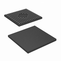
CY7C0851AV-167BBXC Cypress Semiconductor Corp, CY7C0851AV-167BBXC Datasheet - Page 20

CY7C0851AV-167BBXC
Manufacturer Part Number
CY7C0851AV-167BBXC
Description
CY7C0851AV-167BBXC
Manufacturer
Cypress Semiconductor Corp
Datasheet
1.CY7C0851AV-133AXI.pdf
(36 pages)
Specifications of CY7C0851AV-167BBXC
Format - Memory
RAM
Memory Type
SRAM - Dual Port, Synchronous
Memory Size
2M (64K x 36)
Speed
167MHz
Interface
Parallel
Voltage - Supply
3.135 V ~ 3.465 V
Operating Temperature
0°C ~ 70°C
Package / Case
172-LFBGA
Density
2Mb
Access Time (max)
4ns
Sync/async
Synchronous
Architecture
SDR
Clock Freq (max)
167MHz
Operating Supply Voltage (typ)
3.3V
Address Bus
16b
Package Type
FBGA
Operating Temp Range
0C to 70C
Number Of Ports
2
Supply Current
300mA
Operating Supply Voltage (min)
3.135V
Operating Supply Voltage (max)
3.465V
Operating Temperature Classification
Commercial
Mounting
Surface Mount
Pin Count
172
Word Size
36b
Number Of Words
64K
Lead Free Status / RoHS Status
Lead free / RoHS Compliant
Lead Free Status / RoHS Status
Lead free / RoHS Compliant
Available stocks
Company
Part Number
Manufacturer
Quantity
Price
Company:
Part Number:
CY7C0851AV-167BBXC
Manufacturer:
Cypress Semiconductor Corp
Quantity:
10 000
Switching Waveforms
Document #: 38-06070 Rev. *J
Notes
37. Addresses do not have to be accessed sequentially since ADS = CNTEN = V
38. Output state (HIGH, LOW, or high-impedance) is determined by the previous cycle control signals.
39. CE
40. CE
ADDRESS
ADDRESS
Numbers are for reference only
(labelled as no operation). One clock cycle is required to three-state the I/O for the Write operation on the next rising edge of CLK.
DATA
DATA
CNTEN
0
0
DATA
= B0 – B3 = R/W = LOW; CE
= OE = B0 – B3 = LOW; CE
ADS
CLK
OUT
CLK
R/W
OUT
OE
CE
IN
t
t
t
SAD
SCN
SA
t
t
t
SW
SC
SA
Q
A
x–1
n
A
t
EXTERNAL
n
ADDRESS
CH2
t
READ
CH2
1
1
t
CYC2
t
t
= CNTRST = MRST = CNT/MSK = HIGH. When R/W first switches low, since OE = LOW, the Write operation cannot be completed
= R/W = CNTRST = MRST = HIGH.
t
HCN
HAD
t
HA
t
CYC2
t
t
HW
HC
HA
(continued)
Figure 12. Read-to-Write-to-Read (OE Controlled)
t
CL2
t
CL2
Figure 13. Read with Address Counter Advance
Q
A
x
READ
t
n+1
DC
t
CD2
t
CD2
READ WITH COUNTER
Q
t
OHZ
n
t
SW
t
Q
SD
D
A
n
n+2
n+2
t
HW
t
HD
IL
with CNT/MSK = V
CY7C0850AV,CY7C0851V/CY7C0851AV
t
t
SAD
SCN
Q
WRITE
A
D
n+1
COUNTER HOLD
n+3
n+3
IH
constantly loads the address on the rising edge of the CLK.
t
t
HAD
HCN
[37, 38, 39, 40]
CY7C0852V/CY7C0852AV
CY7C0853V/CY7C0853AV
[39]
A
n+4
t
CD2
Q
READ WITH COUNTER
n+2
READ
Q
n+1
A
n+5
t
CD2
Page 20 of 36
Q
n+4
Q
n+3
[+] Feedback


