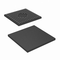
CY7C0851AV-167BBXC Cypress Semiconductor Corp, CY7C0851AV-167BBXC Datasheet - Page 28

CY7C0851AV-167BBXC
Manufacturer Part Number
CY7C0851AV-167BBXC
Description
CY7C0851AV-167BBXC
Manufacturer
Cypress Semiconductor Corp
Datasheet
1.CY7C0851AV-133AXI.pdf
(36 pages)
Specifications of CY7C0851AV-167BBXC
Format - Memory
RAM
Memory Type
SRAM - Dual Port, Synchronous
Memory Size
2M (64K x 36)
Speed
167MHz
Interface
Parallel
Voltage - Supply
3.135 V ~ 3.465 V
Operating Temperature
0°C ~ 70°C
Package / Case
172-LFBGA
Density
2Mb
Access Time (max)
4ns
Sync/async
Synchronous
Architecture
SDR
Clock Freq (max)
167MHz
Operating Supply Voltage (typ)
3.3V
Address Bus
16b
Package Type
FBGA
Operating Temp Range
0C to 70C
Number Of Ports
2
Supply Current
300mA
Operating Supply Voltage (min)
3.135V
Operating Supply Voltage (max)
3.465V
Operating Temperature Classification
Commercial
Mounting
Surface Mount
Pin Count
172
Word Size
36b
Number Of Words
64K
Lead Free Status / RoHS Status
Lead free / RoHS Compliant
Lead Free Status / RoHS Status
Lead free / RoHS Compliant
Available stocks
Company
Part Number
Manufacturer
Quantity
Price
Company:
Part Number:
CY7C0851AV-167BBXC
Manufacturer:
Cypress Semiconductor Corp
Quantity:
10 000
Switching Waveforms
Table 7. Read/Write and Enable Operation (Any Port)
Notes
Document #: 38-06070 Rev. *J
57. CE
58. Address “3FFFF” is the mailbox location for R_Port of a 9M device.
59. L_Port is configured for Write operation, and R_Port is configured for Read operation.
60. At least one byte enable (B0 – B3) is required to be active during interrupt operations.
61. Interrupt flag is set with respect to the rising edge of the Write clock, and is reset with respect to the rising edge of the Read clock.
62. OE is an asynchronous input signal.
63. When CE changes state, deselection and Read happen after one cycle of latency.
64. 9 M device has 18 address bits, 4M device has 17 address bits, 2 M device has 16 address bits, and 1M device has 15 address bits.
65. “X” = “Don’t Care,” “H” = HIGH, “L” = LOW.
CLK
L_PORT
ADDRESS
INT
CLK
R_PORT
ADDRESS
OE
H
X
X
X
L
0
R
= OE = ADS = CNTEN = LOW; CE
L
R
CLK
X
t
CH2
t
CH2
t
CYC2
Inputs
t
CYC2
CE
t
(continued)
CL2
H
X
L
L
L
1
t
t
0
SA
3FFFF
= CNTRST = MRST = CNT/MSK = HIGH.
CL2
t
SA
Figure 23. MailBox Interrupt Timing
A
t
HA
m
t
t
HA
SINT
CE
X
H
H
H
L
1
A
n
A
[64, 65, 62, 63]
R/W
m+1
X
X
H
X
L
CY7C0850AV,CY7C0851V/CY7C0851AV
A
n+1
3FFFF
DQ
Outputs
High-Z
High-Z
High-Z
[57, 58, 59, 60, 61]
D
0
D
OUT
– DQ
IN
t
RINT
35
CY7C0852V/CY7C0852AV
CY7C0853V/CY7C0853AV
A
n+2
A
Deselected
Deselected
Write
Read
Outputs disabled
m+3
Operation
A
n+3
A
m+4
Page 28 of 36
[+] Feedback


