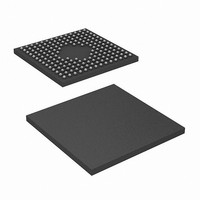
CY7C0853V-100BBC Cypress Semiconductor Corp, CY7C0853V-100BBC Datasheet - Page 17

CY7C0853V-100BBC
Manufacturer Part Number
CY7C0853V-100BBC
Description
IC,SYNC SRAM,256KX36,CMOS,BGA,172PIN,PLASTIC
Manufacturer
Cypress Semiconductor Corp
Datasheet
1.CY7C0853V-100BBC.pdf
(29 pages)
Specifications of CY7C0853V-100BBC
Format - Memory
RAM
Memory Type
SRAM - Dual Port, Synchronous
Memory Size
9M (256K x 36)
Speed
100MHz
Interface
Parallel
Voltage - Supply
3.135 V ~ 3.465 V
Operating Temperature
0°C ~ 70°C
Package / Case
172-LFBGA
Lead Free Status / RoHS Status
Contains lead / RoHS non-compliant
Available stocks
Company
Part Number
Manufacturer
Quantity
Price
Company:
Part Number:
CY7C0853V-100BBC
Manufacturer:
CY
Quantity:
19
Company:
Part Number:
CY7C0853V-100BBC
Manufacturer:
Cypress Semiconductor Corp
Quantity:
10 000
Document #: 38-06070 Rev. *D
Switching Waveforms
Read Cycle
Notes:
22. OE is asynchronously controlled; all other inputs (excluding MRST and JTAG) are synchronous to the rising clock edge.
23. ADS = CNTEN = LOW, and MRST = CNTRST = CNT/MSK = HIGH.
24. The output is disabled (high-impedance state) by CE = V
25. Addresses do not have to be accessed sequentially since ADS = CNTEN = V
Master Reset
MRST
ALL
ADDRESS/
DATA
LINES
ALL
OTHER
INPUTS
TMS
CNTINT
INT
TDO
Numbers are for reference only.
ADDRESS
DATA
B0–B3
R/W
CLK
OUT
OE
[ 4, 22, 23, 24, 25]
CE
t
RSF
t
t
t
t
SB
SW
SA
SC
A
t
RS
n
t
t
t
t
INACTIVE
RSS
t
HB
HW
HA
t
HC
CH2
1 Latency
t
RSR
t
CYC2
t
CKLZ
t
CL2
IH
A
n+1
following the next rising edge of the clock.
ACTIVE
t
CD2
IL
with CNT/MSK = V
Q
A
n
n+2
IH
constantly loads the address on the rising edge of the CLK.
t
DC
CY7C0850V/CY7C0851V
CY7C0852V/CY7C0853V
Q
t
SC
n+1
t
OHZ
A
n+3
t
OLZ
t
HC
t
OE
Page 17 of 29
Q
n+2


