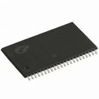
CY7C1041D-10ZSXIT Cypress Semiconductor Corp, CY7C1041D-10ZSXIT Datasheet - Page 6

CY7C1041D-10ZSXIT
Manufacturer Part Number
CY7C1041D-10ZSXIT
Description
CY7C1041D-10ZSXIT
Manufacturer
Cypress Semiconductor Corp
Specifications of CY7C1041D-10ZSXIT
Format - Memory
RAM
Memory Type
SRAM - Asynchronous
Memory Size
4M (256K x 16)
Speed
10ns
Interface
Parallel
Voltage - Supply
4.5 V ~ 5.5 V
Operating Temperature
-40°C ~ 85°C
Package / Case
44-TSOP II
Density
4Mb
Access Time (max)
10ns
Sync/async
Asynchronous
Architecture
Not Required
Clock Freq (max)
Not RequiredMHz
Operating Supply Voltage (typ)
5V
Address Bus
18b
Package Type
TSOP-II
Operating Temp Range
-40C to 85C
Number Of Ports
1
Supply Current
90mA
Operating Supply Voltage (min)
4.5V
Operating Supply Voltage (max)
5.5V
Operating Temperature Classification
Industrial
Mounting
Surface Mount
Pin Count
44
Word Size
16b
Number Of Words
256K
Lead Free Status / RoHS Status
Lead free / RoHS Compliant
Lead Free Status / RoHS Status
Lead free / RoHS Compliant
Switching Characteristics
Data Retention Characteristics
Data Retention Waveform
Document #: 38-05472 Rev. *F
Notes
Write Cycle
t
t
t
t
t
t
t
t
t
t
t
V
I
I
t
t
WC
SCE
AW
HA
SA
PWE
SD
HD
LZWE
HZWE
BW
CCDR
CCDR
CDR
R
10. The internal Write time of the memory is defined by the overlap of CE LOW, and WE LOW. CE and WE must be LOW to initiate a Write, and the transition of either
11. The minimum Write cycle time for Write Cycle No. 3 (WE controlled, OE LOW) is the sum of t
12. Full device operation requires linear V
13. No input may exceed V
14. Device is continuously selected. OE, CE, BHE, and/or BHE = V
DR
[12]
Parameter
of these signals can terminate the Write. The input data set-up and hold timing should be referenced to the leading edge of the signal that terminates the Write.
Parameter
[4]
V
CE
CC
[10, 11]
V
Data Retention Current
Data Retention Current
Chip Deselect to Data Retention Time
Operation Recovery Time
CC
Write Cycle Time
CE LOW to Write End
Address Set-Up to Write End
Address Hold from Write End
Address Set-Up to Write Start
WE Pulse Width
Data Set-Up to Write End
Data Hold from Write End
WE HIGH to Low Z
WE LOW to High Z
Byte Enable to End of Write
for Data Retention
CC
+ 0.5 V
Description
CC
ramp from V
[6]
Description
[9]
[8, 9]
Over the Operating Range(continued)
t
CDR
4.5 V
Over the Operating Range
DR
to V
CC(Min)
IL
.
V
CE > V
V
> 50 μs or stable at V
CC
IN
DATA RETENTION MODE
> V
= V
CC
CC
DR
– 0.3 V,
– 0.3 V or V
= 2.0 V,
V
DR
Conditions
> 2 V
Min
–10 (Industrial)
10
CC(Min)
7
7
0
0
7
3
6
0
7
HZWE
IN
> 50 μs
< 0.3 V
and t
[13]
SD
Max
.
5
Auto
Ind’l
4.5 V
–12 (Automotive)
t
R
Min
12
10
10
10
10
0
0
7
0
3
Min
2.0
t
RC
0
Max
Max
CY7C1041D
10
15
6
Page 6 of 14
Unit
mA
mA
ns
ns
V
Unit
ns
ns
ns
ns
ns
ns
ns
ns
ns
ns
ns
[+] Feedback


