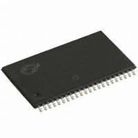
CY7C1041D-10ZSXIT Cypress Semiconductor Corp, CY7C1041D-10ZSXIT Datasheet - Page 3

CY7C1041D-10ZSXIT
Manufacturer Part Number
CY7C1041D-10ZSXIT
Description
CY7C1041D-10ZSXIT
Manufacturer
Cypress Semiconductor Corp
Specifications of CY7C1041D-10ZSXIT
Format - Memory
RAM
Memory Type
SRAM - Asynchronous
Memory Size
4M (256K x 16)
Speed
10ns
Interface
Parallel
Voltage - Supply
4.5 V ~ 5.5 V
Operating Temperature
-40°C ~ 85°C
Package / Case
44-TSOP II
Density
4Mb
Access Time (max)
10ns
Sync/async
Asynchronous
Architecture
Not Required
Clock Freq (max)
Not RequiredMHz
Operating Supply Voltage (typ)
5V
Address Bus
18b
Package Type
TSOP-II
Operating Temp Range
-40C to 85C
Number Of Ports
1
Supply Current
90mA
Operating Supply Voltage (min)
4.5V
Operating Supply Voltage (max)
5.5V
Operating Temperature Classification
Industrial
Mounting
Surface Mount
Pin Count
44
Word Size
16b
Number Of Words
256K
Lead Free Status / RoHS Status
Lead free / RoHS Compliant
Lead Free Status / RoHS Status
Lead free / RoHS Compliant
Document #: 38-05472 Rev. *E
Thermal Resistance
AC Test Loads and Waveforms
Switching Characteristics
Read Cycle
t
t
t
t
t
t
t
t
t
t
t
t
t
t
t
Notes:
power
RC
AA
OHA
ACE
DOE
LZOE
HZOE
LZCE
HZCE
PU
PD
DBE
LZBE
HZBE
5. AC characteristics (except High-Z) are tested using the load conditions shown in Figure (a). High-Z characteristics are tested for all speeds using the test load
6. Test conditions assume signal transition time of 3 ns or less, timing reference levels of 1.5V, input pulse levels of 0 to 3.0V, and output loading of the specified
7. t
8. t
9. At any given temperature and voltage condition, t
Parameter
shown in Figure (c)
I
Parameter
OL
POWER
HZOE
* CAPACITIVE LOAD CONSISTS
OF ALL COMPONENTS OF THE
TEST ENVIRONMENT
/I
OH
10 ns device
JA
JC
, t
HZCE
and 30-pF load capacitance.
gives the minimum amount of time that the power supply should be at typical V
, t
OUTPUT
HZBE
Thermal Resistance
(Junction to Ambient)
Thermal Resistance
(Junction to Case)
, and t
OUTPUT
V
Read Cycle Time
Address to Data Valid
Data Hold from Address Change
CE LOW to Data Valid
OE LOW to Data Valid
OE LOW to Low Z
OE HIGH to High Z
CE LOW to Low Z
CE HIGH to High Z
CE LOW to Power-Up
CE HIGH to Power-Down
Byte Enable to Data Valid
Byte Enable to Low Z
Byte Disable to High Z
High-Z Characteristics:
CC
HZWE
INCLUDING
JIG AND
SCOPE
(typical) to the First Access
Description
5V
are specified with a load capacitance of 5 pF as in part (c) of AC Test Loads. Transition is measured when the outputs enter a high impedance state.
[4]
Z = 50
5 pF
[6]
[4]
Description
R1 481
Over the Operating Range
[9]
[4]
[8, 9]
[8, 9]
(a)
1.5V
50
[5]
HZCE
(c)
is less than t
Still Air, soldered on a 3 × 4.5 inch,
four-layer printed circuit board
255
R2
[7]
30 pF*
LZCE
Test Conditions
, t
HZOE
is less than t
Equivalent to:
Min.
GND
100
3.0V
-10 (Industrial)
10
3
0
3
0
0
CC
LZOE
3 ns
values until the first memory access can be performed.
, t
OUTPUT
HZBE
is less than t
Max.
10
10
10
5
5
5
5
5
SOJ Package TSOP II Package
THÉ
10%
VENIN EQUIVALENT
LZBE,
57.91
36.73
90%
ALL INPUT PULSES
167
and t
(b)
-12 (Automotive)
Min.
100
HZWE
12
3
0
3
0
0
is less than t
1.73V
CY7C1041D
50.66
17.17
Max.
12
12
12
6
6
6
6
6
LZWE
90%
for any given device.
Page 3 of 11
10%
3 ns
Unit
s
ns
ns
ns
ns
ns
ns
ns
ns
ns
ns
ns
ns
ns
ns
C/W
C/W
Unit
[+] Feedback


