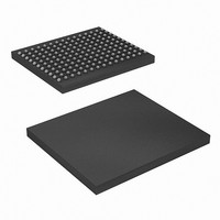
CY7C1354CV25-166BZC Cypress Semiconductor Corp, CY7C1354CV25-166BZC Datasheet - Page 15

CY7C1354CV25-166BZC
Manufacturer Part Number
CY7C1354CV25-166BZC
Description
CY7C1354CV25-166BZC
Manufacturer
Cypress Semiconductor Corp
Datasheet
1.CY7C1354CV25-200AXC.pdf
(30 pages)
Specifications of CY7C1354CV25-166BZC
Format - Memory
RAM
Memory Type
SRAM - Synchronous
Memory Size
9M (256K x 36)
Speed
166MHz
Interface
Parallel
Voltage - Supply
2.375 V ~ 2.625 V
Operating Temperature
0°C ~ 70°C
Package / Case
165-LFBGA
Lead Free Status / RoHS Status
Contains lead / RoHS non-compliant
Available stocks
Company
Part Number
Manufacturer
Quantity
Price
Company:
Part Number:
CY7C1354CV25-166BZC
Manufacturer:
Cypress Semiconductor Corp
Quantity:
10 000
Company:
Part Number:
CY7C1354CV25-166BZCT
Manufacturer:
Cypress Semiconductor Corp
Quantity:
10 000
2.5 V TAP AC Test Conditions
Input pulse levels ...............................................V
Input rise and fall time ....................................................1 ns
Input timing reference levels ....................................... 1.25 V
Output reference levels .............................................. 1.25 V
Test load termination supply voltage ................... ........1.25 V
TAP DC Electrical Characteristics And Operating Conditions
(0 °C < T
Identification Register Definitions
Scan Register Sizes
Identification Codes
Document Number: 38-05537 Rev. *K
V
V
V
V
V
V
I
Revision number (31:29)
Cypress device ID (28:12)
Cypress JEDEC ID (11:1)
ID register presence (0)
Instruction
Bypass
ID
Boundary scan order (119-ball BGA package)
Boundary scan order (165-ball FBGA package)
EXTEST
IDCODE
SAMPLE Z
RESERVED
SAMPLE/PRELOAD 100
RESERVED
RESERVED
BYPASS
Note
X
16. All voltages referenced to V
OH1
OH2
OL1
OL2
IH
IL
Parameter
Instruction
Instruction Field
A
< +70 °C; V
Register Name
Output HIGH voltage
Output HIGH voltage
Output LOW voltage
Output LOW voltage
Input HIGH voltage
Input LOW voltage
Input Load current
DD
000
001
010
011
101
110
111
Code
SS
= 2.5 V ± 0.125 V unless otherwise noted)
Description
(GND).
Captures the input/output ring contents. Places the boundary scan register between the TDI and
TDO. Forces all SRAM outputs to high Z state.
Loads the ID register with the vendor ID code and places the register between TDI and TDO. This
operation does not affect SRAM operation.
Captures the input/output contents. Places the boundary scan register between TDI and TDO.
Forces all SRAM output drivers to a high Z state.
Do Not Use: This instruction is reserved for future use.
Captures the input/output ring contents. Places the boundary scan register between TDI and TDO.
Does not affect the SRAM operation.
Do Not Use: This instruction is reserved for future use.
Do Not Use: This instruction is reserved for future use.
Places the bypass register between TDI and TDO. This operation does not affect SRAM operation.
01011001000100110
CY7C1354CV25
00000110100
000
I
I
I
I
GND < V
1
OH
OH
OL
OL
= 8.0 mA, V
= 100 µA
= –1.0 mA, V
= –100 µA,V
SS
to 2.5 V
IN
< V
Test Conditions
01011001000010110 Reserved for future use.
DDQ
DDQ
DDQ
CY7C1356CV25
Bit Size (× 36)
DDQ
00000110100
= 2.5 V
= 2.5 V
= 2.5 V
32
69
69
000
3
1
[16]
2.5 V TAP AC Output Load Equivalent
V
V
V
1
DDQ
DDQ
DDQ
Description
= 2.5 V
= 2.5 V
= 2.5 V
TDO
Reserved for version number.
Allows unique identification of SRAM vendor.
Indicate the presence of an ID register.
Z = 50Ω
O
–0.3
Min
2.0
2.1
1.7
–5
–
–
Description
Bit Size (× 18)
1.25V
V
CY7C1354CV25
CY7C1356CV25
DD
32
69
69
Max
3
1
0.4
0.2
0.7
20pF
–
–
5
50Ω
+ 0.3
Page 15 of 30
Unit
µA
V
V
V
V
V
V
[+] Feedback


