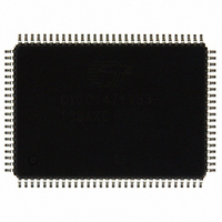
CY7C1471V33-133AXC Cypress Semiconductor Corp, CY7C1471V33-133AXC Datasheet - Page 17

CY7C1471V33-133AXC
Manufacturer Part Number
CY7C1471V33-133AXC
Description
SRAM (Static RAM)
Manufacturer
Cypress Semiconductor Corp
Datasheet
1.CY7C1471V33-133AXC.pdf
(36 pages)
Specifications of CY7C1471V33-133AXC
Format - Memory
RAM
Memory Type
SRAM - Synchronous
Memory Size
72M (2M x 36)
Speed
133MHz
Interface
Parallel
Voltage - Supply
3.135 V ~ 3.6 V
Operating Temperature
0°C ~ 70°C
Package / Case
100-LQFP
Density
72Mb
Access Time (max)
6.5ns
Sync/async
Synchronous
Architecture
SDR
Clock Freq (max)
133MHz
Operating Supply Voltage (typ)
3.3V
Address Bus
21b
Package Type
TQFP
Operating Temp Range
0C to 70C
Number Of Ports
4
Supply Current
305mA
Operating Supply Voltage (min)
3.135V
Operating Supply Voltage (max)
3.6V
Operating Temperature Classification
Commercial
Mounting
Surface Mount
Pin Count
100
Word Size
36b
Number Of Words
2M
Lead Free Status / RoHS Status
Lead free / RoHS Compliant
Lead Free Status / RoHS Status
Lead free / RoHS Compliant
Other names
428-2167
CY7C1471V33-133AXC
CY7C1471V33-133AXC
Available stocks
Company
Part Number
Manufacturer
Quantity
Price
Company:
Part Number:
CY7C1471V33-133AXC
Manufacturer:
Cypress Semiconductor Corp
Quantity:
135
Company:
Part Number:
CY7C1471V33-133AXC
Manufacturer:
TOSHIBA
Quantity:
2 100
Company:
Part Number:
CY7C1471V33-133AXC
Manufacturer:
Cypress Semiconductor Corp
Quantity:
10 000
Part Number:
CY7C1471V33-133AXC
Manufacturer:
CYPRESS/赛普拉斯
Quantity:
20 000
Company:
Part Number:
CY7C1471V33-133AXCT
Manufacturer:
Cypress Semiconductor Corp
Quantity:
10 000
there is no guarantee as to the value that is captured.
Repeatable results may not be possible.
To guarantee that the boundary scan register captures the
correct value of a signal, the SRAM signal must be stabilized
long enough to meet the TAP controller’s capture setup plus hold
time (t
The SRAM clock input might not be captured correctly if there is
no way in a design to stop (or slow) the clock during a
SAMPLE/PRELOAD instruction. If this is an issue, it is still
possible to capture all other signals and simply ignore the value
of the CLK captured in the boundary scan register.
After the data is captured, it is possible to shift out the data by
putting the TAP into the Shift-DR state. This places the boundary
scan register between the TDI and TDO balls.
TAP Timing
Document Number: 38-05288 Rev. *L
CS
plus t
Test M ode Select
CH
).
Test Data-Out
Test Data-In
Test Clock
(TDO)
(TM S)
(TCK )
(TDI)
1
t TM SS
t TDIS
2
t TM SH
t TDIH
t TH
DON’T CA RE
t
TL
3
Note that since the PRELOAD part of the command is not
implemented, putting the TAP to the Update-DR state while
performing a SAMPLE/PRELOAD instruction has the same
effect as the Pause-DR command.
BYPASS
When the BYPASS instruction is loaded in the instruction register
and the TAP is placed in a Shift-DR state, the bypass register is
placed between the TDI and TDO balls. The advantage of the
BYPASS instruction is that it shortens the boundary scan path
when multiple devices are connected together on a board.
Reserved
These instructions are not implemented but are reserved for
future use. Do not use these instructions.
t CY C
UNDEFINED
4
t TDOX
t TDOV
5
6
CY7C1471V33
CY7C1473V33
CY7C1475V33
Page 17 of 36
[+] Feedback


