DG448DV-T1-E3 Vishay, DG448DV-T1-E3 Datasheet
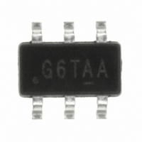
IC,ANALOG SWITCH,SINGLE,SPST,TSOP,6PIN,PLASTIC

DG448DV-T1-E3

Manufacturer Part Number
DG448DV-T1-E3
Description
IC,ANALOG SWITCH,SINGLE,SPST,TSOP,6PIN,PLASTIC
Manufacturer
Vishay
Datasheet

Specifications of DG448DV-T1-E3

Function
Switch
Circuit
2 x SPST - NO
On-state Resistance
25 Ohm
Voltage Supply Source
Single, Dual Supply
Voltage - Supply, Single/dual (±)
7 V ~ 36 V, ± 4.5 V ~ 20 V
Current - Supply
16µA
Operating Temperature
-40°C ~ 85°C
Mounting Type
Surface Mount
Package / Case
6-TSOP (0.063", 1.60mm Width)
Number Of Switches
1
Switch Configuration
SPST
On Resistance (max)
45 Ohms
On Time (max)
175 ns
Off Time (max)
120 ns
Supply Voltage (max)
36 V
Supply Voltage (min)
7 V
Supply Current
0.016 mA
Maximum Power Dissipation
570 mW
Maximum Operating Temperature
+ 85 C
Mounting Style
SMD/SMT
Minimum Operating Temperature
- 40 C
Switch Current (typ)
0.016 mA, - 0.00002 mA
Lead Free Status / RoHS Status
Lead free / RoHS Compliant
Lead Free Status / RoHS Status
Lead free / RoHS Compliant
Other names
DG448DV-T1-E3TR

Available stocks

Company
Part Number
Manufacturer
Quantity
Price
Part Number:
DG448DV-T1-E3
Manufacturer:
Maxim
Quantity:
253
Company:
Part Number:
DG448DV-T1-E3
Quantity:
70 000
DESCRIPTION
The DG447, DG448 are dual supply single-pole/single-throw
(SPST) switches. On resistance is 25 Ω maximum and
flatness is 2.2 Ω max over the specified analog signal range.
These analog switches were designed to provide high
speed, low error switching of precision analog signals. The
primary application areas are in the routing and switching in
telecommunications and test equipment. Combining low
power, low leakages, low on-resistance and small physical
size, the DG477, DG448 are also ideally suited for portable
and battery powered industrial and military equipment.
The DG477 has one normally closed switch, while the
DG448 switch is normally open. They operate either from a
single + 7 V to 36 V supply or from dual ± 4.5 V to ± 20 V
supplies. They are offered in the very popular, small TSOP6
package.
FUNCTIONAL BLOCK DIAGRAM AND PIN CONFIGURATION
Document Number: 73854
S09-1260-Rev. C, 13-Jul-09
NC
NO
IN
IN
V-
V-
Low Power, High Voltage SPST Analog Switches
1
2
3
1
2
3
DG447
DG448
TSOP6
TSOP6
6
5
4
6
5
4
COM
V+
GND
COM
V+
GND
FEATURES
BENEFITS
APPLICATIONS
Logic "0" ≤ 0.8 V
Logic "1" ≥ 2.4 V
Device Marking:
DG447DV = G5xxx
DG448DV = G6xxx
• ± 15 V analog signal range
• On-resistance - R
• Fast switching action - t
• V
• TTL CMOS input compatible
• Rail to rail signal handling
• Dual or single supply operation
• Compliant to RoHS directive 2002/95/EC
• Wide dynamic range
• Low signal errors and distortion
• Break-before-make switching action
• Simple interfacing
• Reduced board space
• Improved reliability
• Precision test equipment
• Precision instrumentation
• Communications systems
• PBX, PABX systems
• Audio equipment
• Redundant systems
• PC multimedia boards
• Hard disc drives
TRUTH TABLE
L
logic supply not required
Logic
0
1
DS(on)
: 25 Ω max.
ON
DG447
OFF
ON
: 100 ns
DG447, DG448
Vishay Siliconix
www.vishay.com
DG448
OFF
ON
1

Related parts for DG448DV-T1-E3

DG448DV-T1-E3 Summary of contents

Page 1

... Redundant systems • PC multimedia boards • Hard disc drives TRUTH TABLE Logic COM Logic "0" ≤ 0.8 V Logic "1" ≥ 2.4 V GND Device Marking: DG447DV = G5xxx DG448DV = G6xxx COM V+ GND DG447, DG448 Vishay Siliconix : 25 Ω max. DS(on) : 100 ns ON DG447 DG448 ON OFF ...

Page 2

... Source Off Capacitance C S(off) e Drain Off Capacitance C D(off) e Channel On Capacitance C D(on) Power Supplies Positive Supply Current I+ Negative Supply Current I- www.vishay.com 2 Package DG447DV-T1-E3 DG448DV-T1- °C, unless otherwise noted A c 6-Pin TSOP Test Conditions Unless Otherwise Specified 2 no/nc COM 13.5 V ± ...

Page 3

... V = no/nc COM 10 mA no/nc COM 300 Ω, C ± NO Ω nF gen gen DG447, DG448 Vishay Siliconix D Suffix - 40 ° ° Temp. Min. Typ. Max. Full 0 V Room 32 Full Room 2 Full Room 140 Full Room 50 Full Room 12 Room 22 Full www.vishay.com d Unit 12 ...

Page 4

... DG447, DG448 Vishay Siliconix TYPICAL CHARACTERISTICS Analog Voltage (V) COM R vs. V and Single Supply Voltage ON COM ± ± ± Analog Voltage (V) COM R vs. V and Dual Supply Voltage ON COM 600 400 200 I COM(OFF NO/NC(OFF) - 200 - 400 - 600 - 16.5 - 13.5 - 10.5 - 7.5 - 4.5 - 1.5 1.5 ...

Page 5

... Temperature (°C) Switching Time vs. Temperature Document Number: 73854 S09-1260-Rev. C, 13-Jul- °C, unless otherwise noted I+, I GND 100 µA 10 µ ± 16 ± DG447, DG448 Vishay Siliconix V = ± ± ± ± µ Vin (V) Supply Current vs 160 140 t ON 120 100 OFF 40 20 ...

Page 6

... DG447, DG448 Vishay Siliconix TYPICAL CHARACTERISTICS T 160 140 120 100 Analog Voltage (V) Charge Injection vs. Analog Voltage (Measured at COM pin) 2.5 2.3 2.1 1.9 1.7 1.5 1.3 1.1 0.9 0.7 0 (V) Input Switching Threshold vs. Supply Voltage TEST CIRCUITS V is the steady state output with the switch on. ...

Page 7

... Figure 3. Off Isolation 0 V 2.4 V Vishay Siliconix maintains worldwide manufacturing capability. Products may be manufactured at one of several qualified locations. Reliability data for Silicon Technology and Package Reliability represent a composite of all qualified locations. For related documents such as package/tape drawings, part marking, and reliability data, see www.vishay.com/ppg?73854. ...

Page 8

... Vishay product could result in personal injury or death. Customers using or selling Vishay products not expressly indicated for use in such applications their own risk and agree to fully indemnify and hold Vishay and its distributors harmless from and against any and all claims, liabilities, expenses and damages arising or resulting in connection with such use or sale, including attorneys fees, even if such claim alleges that Vishay or its distributor was negligent regarding the design or manufacture of the part ...

Related keywords