DG448DV-T1-E3 Vishay, DG448DV-T1-E3 Datasheet - Page 2
DG448DV-T1-E3
Manufacturer Part Number
DG448DV-T1-E3
Description
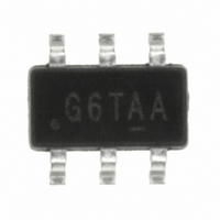
IC,ANALOG SWITCH,SINGLE,SPST,TSOP,6PIN,PLASTIC
Manufacturer
Vishay
Datasheet
1.DG448DV-T1-E3.pdf
(8 pages)
Specifications of DG448DV-T1-E3
Function
Switch
Circuit
2 x SPST - NO
On-state Resistance
25 Ohm
Voltage Supply Source
Single, Dual Supply
Voltage - Supply, Single/dual (±)
7 V ~ 36 V, ± 4.5 V ~ 20 V
Current - Supply
16µA
Operating Temperature
-40°C ~ 85°C
Mounting Type
Surface Mount
Package / Case
6-TSOP (0.063", 1.60mm Width)
Number Of Switches
1
Switch Configuration
SPST
On Resistance (max)
45 Ohms
On Time (max)
175 ns
Off Time (max)
120 ns
Supply Voltage (max)
36 V
Supply Voltage (min)
7 V
Supply Current
0.016 mA
Maximum Power Dissipation
570 mW
Maximum Operating Temperature
+ 85 C
Mounting Style
SMD/SMT
Minimum Operating Temperature
- 40 C
Switch Current (typ)
0.016 mA, - 0.00002 mA
Lead Free Status / RoHS Status
Lead free / RoHS Compliant
Lead Free Status / RoHS Status
Lead free / RoHS Compliant
Other names
DG448DV-T1-E3TR
Available stocks
Company
Part Number
Manufacturer
Quantity
Price
Company:

Part Number:
DG448DV-T1-E3
Manufacturer:
Maxim
Quantity:
253


DG447, DG448
Vishay Siliconix
Notes:
a. Signals on NO, NC, COM, or IN exceeding V+ or V- will be clamped by internal diodes. Limit forward diode current to maximum current ratings.
b. All leads welded or soldered to PC board.
c. Derate 7 mW/°C above 70 °C.
www.vishay.com
2
ORDERING INFORMATION
DG447, DG448
ABSOLUTE MAXIMUM RATINGS T
Parameter Referenced to V-
V+
GND
Digital Inputs
Current , (Any Terminal) Continuous
Current (NO or NC or COM) Pulsed at 1 ms, 10 % Duty Cycle
Storage Temperature
Power Dissipation (Package)
SPECIFICATIONS
Parameter
Analog Switch
Analog Signal Range
Drain-Source
On-Resistance
On-Resistance Flatness
Switch Off Leakage Current
Channel On Leakage Current
Digital Control
Input, High Voltage
Input, Low Voltage
Input Capacitance
Input Current
Dynamic Characteristics
Turn-On Time
Turn-Off Time
Charge Injection
Off-Isolation
Source Off Capacitance
Drain Off Capacitance
Channel On Capacitance
Power Supplies
Positive Supply Current
Negative Supply Current
- 40 °C to 85 °C
Temp. Range
e
a
, V
e
no/nc
e
, V
e
e
COM
e
e
a
b
V
Flatness
Symbol
I
I
I
no/nc(off)
COM(off)
COM(on)
ANALOG
C
C
C
OIRR
R
R
t
6-Pin TSOP
I
I
C
t
OFF
S(off)
D(off)
D(on)
INH
INL
I
ON
I+
Q
ON
ON
IN
I-
Package
IN
A
C
I
no/nc
= 25 °C, unless otherwise noted
L
C
Unless Otherwise Specified
I
no/nc
= 10 nF, V
L
V+ = 13.5 V, V- = - 13.5 V
V+ = 13.5 V, V- = - 13.5 V
= 5 pF, R
V+ = 16.5 V, V- = - 16.5 V
V
V+ = 16.5, V- = - 16.5 V
R
V+ = 16.5 V, V- = - 16.5
= 10 mA, V
COM
V+ = 15 V, V- = - 15 V
L
V
V
= 10 mA, V
V
Test Conditions
= 300 Ω, C
no/nc
V
IN
COM
V
V
= V
no/nc
IN
IN
= 2.4 V, 0.8 V
f = 1 MHz
f = 1 MHz
6-Pin TSOP
gen
L
DG447DV-T1-E3
DG448DV-T1-E3
= 0 or 5 V
=
no/nc
= 0 or 5 V
=
= 50 Ω, f = 1 MHz
=
-/+
±
= 0 V, R
COM
±
15.5 V
=
L
COM
15.5 V
10 V
±
= 35 pF
=
15.5 V
±
c
=
gen
f
5 V, 0 V
10
= 0 Ω
V
or 30 mA, whichever occurs first
(V-) - 2 V to (V+) + 2 V
Temp.
Room
Room
Room
Room
Room
Room
Room
Room
Room
Room
Room
Room
Room
Room
Room
Full
Full
Full
Full
Full
Full
Full
Full
Full
Full
Full
Full
Part Number
- 65 to 150
b
Limit
100
570
44
25
30
Min.
- 15
- 10
- 10
- 10
- 10
2.4
- 1
- 1
- 1
- 1
- 1
d
- 40 °C to 85 °C
S09-1260-Rev. C, 13-Jul-09
D Suffix
Document Number: 73854
- 0.02
Typ.
- 0.1
- 0.1
- 0.1
100
- 72
0.8
17
50
10
19
30
16
5
8
c
Max.
130
140
110
2.2
0.8
15
25
30
10
10
10
95
30
50
3
1
1
1
1
d
Unit
mW
mA
°C
V
Unit
pC
nA
pF
dB
pF
µA
µA
ns
V
Ω
V
Related parts for DG448DV-T1-E3
Image
Part Number
Description
Manufacturer
Datasheet
Request
R

Part Number:
Description:
357-036-542-201 CARDEDGE 36POS DL .156 BLK LOPRO
Manufacturer:
Vishay
Datasheet:
Part Number:
Description:
357-036-542-201 CARDEDGE 36POS DL .156 BLK LOPRO
Manufacturer:
Vishay
Datasheet:
Part Number:
Description:
357-036-542-201 CARDEDGE 36POS DL .156 BLK LOPRO
Manufacturer:
Vishay
Datasheet:
Part Number:
Description:
357-036-542-201 CARDEDGE 36POS DL .156 BLK LOPRO
Manufacturer:
Vishay
Datasheet:
Part Number:
Description:
357-036-542-201 CARDEDGE 36POS DL .156 BLK LOPRO
Manufacturer:
Vishay
Datasheet:
Part Number:
Description:
357-036-542-201 CARDEDGE 36POS DL .156 BLK LOPRO
Manufacturer:
Vishay
Datasheet:
Part Number:
Description:
357-036-542-201 CARDEDGE 36POS DL .156 BLK LOPRO
Manufacturer:
Vishay
Datasheet:
Part Number:
Description:
357-036-542-201 CARDEDGE 36POS DL .156 BLK LOPRO
Manufacturer:
Vishay
Datasheet:
Part Number:
Description:
357-036-542-201 CARDEDGE 36POS DL .156 BLK LOPRO
Manufacturer:
Vishay
Datasheet:
Part Number:
Description:
357-036-542-201 CARDEDGE 36POS DL .156 BLK LOPRO
Manufacturer:
Vishay
Datasheet:
Part Number:
Description:
357-036-542-201 CARDEDGE 36POS DL .156 BLK LOPRO
Manufacturer:
Vishay
Datasheet:
Part Number:
Description:
357-036-542-201 CARDEDGE 36POS DL .156 BLK LOPRO
Manufacturer:
Vishay
Datasheet:
Part Number:
Description:
357-036-542-201 CARDEDGE 36POS DL .156 BLK LOPRO
Manufacturer:
Vishay
Datasheet:
Part Number:
Description:
357-036-542-201 CARDEDGE 36POS DL .156 BLK LOPRO
Manufacturer:
Vishay
Datasheet:
Part Number:
Description:
357-036-542-201 CARDEDGE 36POS DL .156 BLK LOPRO
Manufacturer:
Vishay
Datasheet: