DG448DV-T1-E3 Vishay, DG448DV-T1-E3 Datasheet - Page 3
DG448DV-T1-E3
Manufacturer Part Number
DG448DV-T1-E3
Description
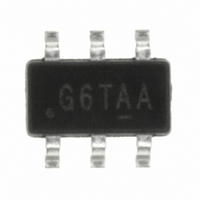
IC,ANALOG SWITCH,SINGLE,SPST,TSOP,6PIN,PLASTIC
Manufacturer
Vishay
Datasheet
1.DG448DV-T1-E3.pdf
(8 pages)
Specifications of DG448DV-T1-E3
Function
Switch
Circuit
2 x SPST - NO
On-state Resistance
25 Ohm
Voltage Supply Source
Single, Dual Supply
Voltage - Supply, Single/dual (±)
7 V ~ 36 V, ± 4.5 V ~ 20 V
Current - Supply
16µA
Operating Temperature
-40°C ~ 85°C
Mounting Type
Surface Mount
Package / Case
6-TSOP (0.063", 1.60mm Width)
Number Of Switches
1
Switch Configuration
SPST
On Resistance (max)
45 Ohms
On Time (max)
175 ns
Off Time (max)
120 ns
Supply Voltage (max)
36 V
Supply Voltage (min)
7 V
Supply Current
0.016 mA
Maximum Power Dissipation
570 mW
Maximum Operating Temperature
+ 85 C
Mounting Style
SMD/SMT
Minimum Operating Temperature
- 40 C
Switch Current (typ)
0.016 mA, - 0.00002 mA
Lead Free Status / RoHS Status
Lead free / RoHS Compliant
Lead Free Status / RoHS Status
Lead free / RoHS Compliant
Other names
DG448DV-T1-E3TR
Available stocks
Company
Part Number
Manufacturer
Quantity
Price
Company:

Part Number:
DG448DV-T1-E3
Manufacturer:
Maxim
Quantity:
253


Notes:
a. Refer to PROCESS OPTION FLOWCHART.
b. Room = 25 °C, Full = as determined by the operating temperature suffix.
c. Typical values are for DESIGN AID ONLY, not guaranteed nor subject to production testing.
d. The algebraic convention whereby the most negative value is a minimum and the most positive a maximum, is used in this data sheet.
e. Guaranteed by design, not subject to production test.
f. V
Stresses beyond those listed under “Absolute Maximum Ratings” may cause permanent damage to the device. These are stress ratings only, and functional operation
of the device at these or any other conditions beyond those indicated in the operational sections of the specifications is not implied. Exposure to absolute maximum
rating conditions for extended periods may affect device reliability.
Document Number: 73854
S09-1260-Rev. C, 13-Jul-09
SPECIFICATIONS
Parameter
Analog Switch
Analog Signal Range
Drain-Source On-Resistance
On-Resistance Flatness
Dynamic Characteristics
Turn-On Time
Turn-Off Time
Charge Injection
Power Supplies
Positive Supply Current
IN
= input voltage to perform proper function.
e
e
a
V
Flatness
Symbol
ANALOG
R
R
t
t
OFF
ON
I+
Q
ON
ON
V
NO, NC
C
I
no/nc
L
Unless Otherwise Specified
I
= 10 nF, V
no/nc
V+ = 13.2 V, V
=
= 10 mA, V
±
V+ = 12 V, V- = 0 V
V
= - 10 mA, V
10 V, R
Test Conditions
IN
V+ = 10.8 V
V+ = 10.8 V
= 2.4 V, 0.8 V
gen
L
= 0 V, R
COM
= 300 Ω, C
IN
= 0 V, 5 V
COM
=
2, 6, 8 V
gen
f
=
8
L
= 0 Ω
=
V
35 pF
Temp.
Room
Room
Room
Room
Room
Room
Full
Full
Full
Full
Full
Full
b
Min.
0
d
DG447, DG448
- 40 °C to 85 °C
D Suffix
Vishay Siliconix
Typ.
140
32
50
12
22
2
c
www.vishay.com
Max.
175
225
120
150
12
45
60
50
75
6
8
d
Unit
pC
nS
µA
Ω
Ω
V
3
Related parts for DG448DV-T1-E3
Image
Part Number
Description
Manufacturer
Datasheet
Request
R

Part Number:
Description:
357-036-542-201 CARDEDGE 36POS DL .156 BLK LOPRO
Manufacturer:
Vishay
Datasheet:
Part Number:
Description:
357-036-542-201 CARDEDGE 36POS DL .156 BLK LOPRO
Manufacturer:
Vishay
Datasheet:
Part Number:
Description:
357-036-542-201 CARDEDGE 36POS DL .156 BLK LOPRO
Manufacturer:
Vishay
Datasheet:
Part Number:
Description:
357-036-542-201 CARDEDGE 36POS DL .156 BLK LOPRO
Manufacturer:
Vishay
Datasheet:
Part Number:
Description:
357-036-542-201 CARDEDGE 36POS DL .156 BLK LOPRO
Manufacturer:
Vishay
Datasheet:
Part Number:
Description:
357-036-542-201 CARDEDGE 36POS DL .156 BLK LOPRO
Manufacturer:
Vishay
Datasheet:
Part Number:
Description:
357-036-542-201 CARDEDGE 36POS DL .156 BLK LOPRO
Manufacturer:
Vishay
Datasheet:
Part Number:
Description:
357-036-542-201 CARDEDGE 36POS DL .156 BLK LOPRO
Manufacturer:
Vishay
Datasheet:
Part Number:
Description:
357-036-542-201 CARDEDGE 36POS DL .156 BLK LOPRO
Manufacturer:
Vishay
Datasheet:
Part Number:
Description:
357-036-542-201 CARDEDGE 36POS DL .156 BLK LOPRO
Manufacturer:
Vishay
Datasheet:
Part Number:
Description:
357-036-542-201 CARDEDGE 36POS DL .156 BLK LOPRO
Manufacturer:
Vishay
Datasheet:
Part Number:
Description:
357-036-542-201 CARDEDGE 36POS DL .156 BLK LOPRO
Manufacturer:
Vishay
Datasheet:
Part Number:
Description:
357-036-542-201 CARDEDGE 36POS DL .156 BLK LOPRO
Manufacturer:
Vishay
Datasheet:
Part Number:
Description:
357-036-542-201 CARDEDGE 36POS DL .156 BLK LOPRO
Manufacturer:
Vishay
Datasheet:
Part Number:
Description:
357-036-542-201 CARDEDGE 36POS DL .156 BLK LOPRO
Manufacturer:
Vishay
Datasheet: