DSPIC33FJ12MC201-E/P Microchip Technology, DSPIC33FJ12MC201-E/P Datasheet - Page 106
DSPIC33FJ12MC201-E/P
Manufacturer Part Number
DSPIC33FJ12MC201-E/P
Description
12 KB Flash, 1 KB RAM, 40 MIPS, 13 I/O, 16-bit Motor Control DSC, NanoWatt 20 PD
Manufacturer
Microchip Technology
Series
dsPIC™ 33Fr
Datasheets
1.PIC24HJ12GP201-ISO.pdf
(84 pages)
2.DSPIC33FJ12MC201-ISO.pdf
(288 pages)
3.DSPIC33FJ12MC201-ISO.pdf
(14 pages)
Specifications of DSPIC33FJ12MC201-E/P
Core Processor
dsPIC
Core Size
16-Bit
Speed
40 MIPs
Connectivity
I²C, IrDA, SPI, UART/USART
Peripherals
Brown-out Detect/Reset, Motor Control PWM, QEI, POR, PWM, WDT
Number Of I /o
15
Program Memory Size
12KB (12K x 8)
Program Memory Type
FLASH
Ram Size
1K x 8
Voltage - Supply (vcc/vdd)
3 V ~ 3.6 V
Data Converters
A/D 4x10b
Oscillator Type
Internal
Operating Temperature
-40°C ~ 125°C
Package / Case
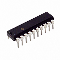
20-DIP (0.300", 7.62mm)
Lead Free Status / RoHS Status
Lead free / RoHS Compliant
For Use With
DV164033 - KIT START EXPLORER 16 MPLAB ICD2DM240001 - BOARD DEMO PIC24/DSPIC33/PIC32
Eeprom Size
-
Lead Free Status / RoHS Status
Lead free / RoHS Compliant


dsPIC33FJ12MC201/202
REGISTER 8-1:
DS70265D-page 104
bit 2
bit 1
bit 0
Note 1: Writes to this register require an unlock sequence. Refer to Section 7. “Oscillator” (DS70227) in the
2: Direct clock switches between any primary oscillator mode with PLL and FRCPLL mode are not permitted.
“PIC24H Family Reference Manual” (available from the Microchip web site) for details.
This applies to clock switches in either direction. In these instances, the application must switch to FRC mode
as a transition clock source between the two PLL modes.
Unimplemented: Read as ‘0’
LPOSCEN: Secondary (LP) Oscillator Enable bit
1 = Enable secondary oscillator
0 = Disable secondary oscillator
OSWEN: Oscillator Switch Enable bit
1 = Request oscillator switch to selection specified by NOSC<2:0> bits
0 = Oscillator switch is complete
OSCCON: OSCILLATOR CONTROL REGISTER
Preliminary
(1)
(CONTINUED)
© 2009 Microchip Technology Inc.
Related parts for DSPIC33FJ12MC201-E/P
Image
Part Number
Description
Manufacturer
Datasheet
Request
R

Part Number:
Description:
IC, DSC, 16BIT, 12KB, 40MHZ, 3.6V, DIP28
Manufacturer:
Microchip Technology
Datasheet:

Part Number:
Description:
Manufacturer:
Microchip Technology Inc.
Datasheet:
Part Number:
Description:
Manufacturer:
Microchip Technology Inc.
Datasheet:
Part Number:
Description:
Manufacturer:
Microchip Technology Inc.
Datasheet:
Part Number:
Description:
Manufacturer:
Microchip Technology Inc.
Datasheet:
Part Number:
Description:
Manufacturer:
Microchip Technology Inc.
Datasheet:
Part Number:
Description:
Manufacturer:
Microchip Technology Inc.
Datasheet:
Part Number:
Description:
Manufacturer:
Microchip Technology Inc.
Datasheet:
Part Number:
Description:
Manufacturer:
Microchip Technology Inc.
Datasheet: