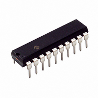
DSPIC33FJ12MC201-E/P Microchip Technology, DSPIC33FJ12MC201-E/P Datasheet - Page 56

DSPIC33FJ12MC201-E/P
Manufacturer Part Number
DSPIC33FJ12MC201-E/P
Description
12 KB Flash, 1 KB RAM, 40 MIPS, 13 I/O, 16-bit Motor Control DSC, NanoWatt 20 PD
Manufacturer
Microchip Technology
Series
dsPIC™ 33Fr
Datasheets
1.PIC24HJ12GP201-ISO.pdf
(84 pages)
2.DSPIC33FJ12MC201-ISO.pdf
(288 pages)
3.DSPIC33FJ12MC201-ISO.pdf
(14 pages)
Specifications of DSPIC33FJ12MC201-E/P
Core Processor
dsPIC
Core Size
16-Bit
Speed
40 MIPs
Connectivity
I²C, IrDA, SPI, UART/USART
Peripherals
Brown-out Detect/Reset, Motor Control PWM, QEI, POR, PWM, WDT
Number Of I /o
15
Program Memory Size
12KB (12K x 8)
Program Memory Type
FLASH
Ram Size
1K x 8
Voltage - Supply (vcc/vdd)
3 V ~ 3.6 V
Data Converters
A/D 4x10b
Oscillator Type
Internal
Operating Temperature
-40°C ~ 125°C
Package / Case
20-DIP (0.300", 7.62mm)
Lead Free Status / RoHS Status
Lead free / RoHS Compliant
For Use With
DV164033 - KIT START EXPLORER 16 MPLAB ICD2DM240001 - BOARD DEMO PIC24/DSPIC33/PIC32
Eeprom Size
-
Lead Free Status / RoHS Status
Lead free / RoHS Compliant
- PIC24HJ12GP201-ISO PDF datasheet
- DSPIC33FJ12MC201-ISO PDF datasheet #2
- DSPIC33FJ12MC201-ISO PDF datasheet #3
- Current page: 56 of 288
- Download datasheet (5Mb)
dsPIC33FJ12MC201/202
5.2
The dsPIC33FJ12MC201/202 Flash program memory
array is organized into rows of 64 instructions or 192
bytes. RTSP allows the user application to erase a
page of memory, which consists of eight rows (512
instructions); and to program one row or one word.
Table 24-12 shows typical erase and programming
times. The 8-row erase pages and single row write
rows are edge-aligned from the beginning of program
memory, on boundaries of 1536 bytes and 192 bytes,
respectively.
The program memory implements holding buffers that
can contain 64 instructions of programming data. Prior
to the actual programming operation, the write data
must be loaded into the buffers sequentially. The
instruction words loaded must always be from a group
of 64 boundary.
The basic sequence for RTSP programming is to set up
a Table Pointer, then do a series of TBLWT instructions
to load the buffers. Programming is performed by
setting the control bits in the NVMCON register. A total
of 64 TBLWTL and TBLWTH instructions are required
to load the instructions.
All of the table write operations are single-word writes
(two instruction cycles) because only the buffers are
written.
programming each row.
DS70265D-page 54
RTSP Operation
A
programming
cycle
is
required
Preliminary
for
5.3
A complete programming sequence is necessary for
programming or erasing the internal Flash in RTSP
mode. The processor stalls (waits) until the operation is
finished.
The programming time depends on the FRC accuracy
(see Table 24-18) and the value of the FRC Oscillator
Tuning register (see Register 8-4). Use the following
formula to calculate the minimum and maximum values
for the Row Write Time, Page Erase Time, and Word
Write Cycle Time parameters (see Table 24-12).
EQUATION 5-1:
For example, if the device is operating at +125°C,
the FRC accuracy will be ±5%. If the TUN<5:0> bits
(see Register 8-4) are set to ‘b111111, the
Minimum Row Write Time is:
and, the Maximum Row Write Time is:
Setting the WR bit (NVMCON<15>) starts the opera-
tion, and the WR bit is automatically cleared when the
operation is finished.
5.4
Two SFRs are used to read and write the program
Flash memory: NVMCON and NVMKEY.
The NVMCON register (Register 5-1) controls which
blocks are to be erased, which memory type is to be
programmed, and the start of the programming cycle.
NVMKEY is a write-only register that is used for write
protection. To start a programming or erase sequence,
the user application must consecutively write 0x55 and
0xAA to the NVMKEY register. Refer to Section 5.3
“Programming Operations” for further details.
T
T
RW
RW
------------------------------------------------------------------------------------------------------------------------- -
7.37 MHz
=
=
--------------------------------------------------------------------------------------------- - 1.586ms
7.37 MHz
--------------------------------------------------------------------------------------------- - 1.435ms
7.37 MHz
Programming Operations
Control Registers
×
(
FRC Accuracy
×
×
(
(
11064 Cycles
11064 Cycles
1 0.05
1
–
+
PROGRAMMING TIME
© 2009 Microchip Technology Inc.
0.05
T
)
)
×
×
)%
(
(
1 0.00375
1 0.00375
×
–
–
(
FRC Tuning
)
)
=
=
)%
Related parts for DSPIC33FJ12MC201-E/P
Image
Part Number
Description
Manufacturer
Datasheet
Request
R

Part Number:
Description:
IC, DSC, 16BIT, 12KB, 40MHZ, 3.6V, DIP28
Manufacturer:
Microchip Technology
Datasheet:

Part Number:
Description:
Manufacturer:
Microchip Technology Inc.
Datasheet:

Part Number:
Description:
Manufacturer:
Microchip Technology Inc.
Datasheet:

Part Number:
Description:
Manufacturer:
Microchip Technology Inc.
Datasheet:

Part Number:
Description:
Manufacturer:
Microchip Technology Inc.
Datasheet:

Part Number:
Description:
Manufacturer:
Microchip Technology Inc.
Datasheet:

Part Number:
Description:
Manufacturer:
Microchip Technology Inc.
Datasheet:

Part Number:
Description:
Manufacturer:
Microchip Technology Inc.
Datasheet:

Part Number:
Description:
Manufacturer:
Microchip Technology Inc.
Datasheet:


