DSPIC33FJ16GS504-I/TL Microchip Technology, DSPIC33FJ16GS504-I/TL Datasheet - Page 249
DSPIC33FJ16GS504-I/TL
Manufacturer Part Number
DSPIC33FJ16GS504-I/TL
Description
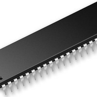
16 Bit MCU/DSP 40MIPS 16 KB FLASH 2KB RAM SMPS 44 TLA 6x6x0.9 Mm TUBE
Manufacturer
Microchip Technology
Series
dsPIC™ 33Fr
Datasheet
1.DSPIC33FJ06GS101-ISO.pdf
(346 pages)
Specifications of DSPIC33FJ16GS504-I/TL
Core Processor
dsPIC
Core Size
16-Bit
Speed
40 MIPs
Connectivity
I²C, IrDA, LIN, SPI, UART/USART
Peripherals
Brown-out Detect/Reset, POR, PWM, WDT
Number Of I /o
35
Program Memory Size
16KB (16K x 8)
Program Memory Type
FLASH
Ram Size
2K x 16
Voltage - Supply (vcc/vdd)
3 V ~ 3.6 V
Data Converters
A/D 12x10b, D/A 1x10b
Oscillator Type
Internal
Operating Temperature
-40°C ~ 85°C
Package / Case
*
Processor Series
dsPIC33FJ
Core
dsPIC
Data Bus Width
16 bit
Data Ram Size
2 KB
Interface Type
I2C, SPI, UART
Maximum Clock Frequency
40 MHz
Number Of Programmable I/os
35
Operating Supply Voltage
3 V to 3.6 V
Maximum Operating Temperature
+ 85 C
Mounting Style
Through Hole
Development Tools By Supplier
DM240001, DM240002
Lead Free Status / RoHS Status
Lead free / RoHS Compliant
Eeprom Size
-
Lead Free Status / Rohs Status
Details


REGISTER 19-2:
© 2009 Microchip Technology Inc.
bit 15
bit 7
Legend:
R = Readable bit
-n = Value at POR
C = Clearable bit
bit 15-7
bit 6
bit 5
bit 4
bit 3
bit 2
bit 1
bit 0
Note 1: This bit is available in the dsPIC33FJ16GS502, dsPIC33FJ16GS504 and dsPIC33FJ06GS202 devices
U-0
U-0
—
—
2: This bit is available in the dsPIC33FJ16GS504 devices only.
3: This bit is available in the dsPIC33FJ16GS402/404, dsPIC33FJ16GS502, dsPIC33FJ16GS504 and
4: This bit is available in the dsPIC33FJ16GS504 and dsPIC33FJ16GS502 devices only.
only.
dsPIC33FJ06GS101 devices only.
Unimplemented: Read as ‘0’
P6RDY: Conversion Data for Pair 6 Ready bit
Bit is set when data is ready in buffer, cleared when a ‘0’ is written to this bit.
P5RDY: Conversion Data for Pair 5 Ready bit
Bit is set when data is ready in buffer, cleared when a ‘0’ is written to this bit.
P4RDY: Conversion Data for Pair 4 Ready bit
Bit is set when data is ready in buffer, cleared when a ‘0’ is written to this bit.
P3RDY: Conversion Data for Pair 3 Ready bit
Bit is set when data is ready in buffer, cleared when a ‘0’ is written to this bit.
P2RDY: Conversion Data for Pair 2 Ready bit
Bit is set when data is ready in buffer, cleared when a ‘0’ is written to this bit.
P1RDY: Conversion Data for Pair 1 Ready bit
Bit is set when data is ready in buffer, cleared when a ‘0’ is written to this bit.
P0RDY: Conversion Data for Pair 0 Ready bit
Bit is set when data is ready in buffer, cleared when a ‘0’ is written to this bit.
dsPIC33FJ06GS101/X02 and dsPIC33FJ16GSX02/X04
R/C-0, HS
P6RDY
U-0
—
ADSTAT: A/D STATUS REGISTER
(1)
W = Writable bit
‘1’ = Bit is set
HS = Hardware Settable bit
R/C-0, HS
P5RDY
U-0
—
(2)
R/C-0, HS
P4RDY
Preliminary
U-0
—
(2)
U = Unimplemented bit, read as ‘0’
‘0’ = Bit is cleared
(1)
(2)
(2)
(3)
(4)
R/C-0, HS
P3RDY
U-0
—
(3)
R/C-0, HS
P2RDY
U-0
—
(4)
x = Bit is unknown
R/C-0, HS
P1RDY
U-0
—
DS70318D-page 247
R/C-0, HS
P0RDY
U-0
—
bit 8
bit 0
Related parts for DSPIC33FJ16GS504-I/TL
Image
Part Number
Description
Manufacturer
Datasheet
Request
R

Part Number:
Description:
IC, DSC, 16BIT, 12KB, 40MHZ, 3.6V, DIP28
Manufacturer:
Microchip Technology
Datasheet:

Part Number:
Description:
Manufacturer:
Microchip Technology Inc.
Datasheet:
Part Number:
Description:
Manufacturer:
Microchip Technology Inc.
Datasheet:
Part Number:
Description:
Manufacturer:
Microchip Technology Inc.
Datasheet:
Part Number:
Description:
Manufacturer:
Microchip Technology Inc.
Datasheet:
Part Number:
Description:
Manufacturer:
Microchip Technology Inc.
Datasheet:
Part Number:
Description:
Manufacturer:
Microchip Technology Inc.
Datasheet:
Part Number:
Description:
Manufacturer:
Microchip Technology Inc.
Datasheet:
Part Number:
Description:
Manufacturer:
Microchip Technology Inc.
Datasheet: