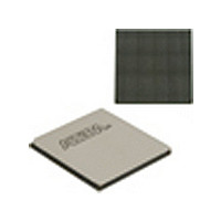
EP2SGX90EF1152I4 Altera, EP2SGX90EF1152I4 Datasheet - Page 157

EP2SGX90EF1152I4
Manufacturer Part Number
EP2SGX90EF1152I4
Description
Stratix II GX
Manufacturer
Altera
Datasheet
1.EP2SGX90EF1152I4.pdf
(316 pages)
Specifications of EP2SGX90EF1152I4
Family Name
Stratix II GX
Number Of Logic Blocks/elements
90960
# I/os (max)
558
Frequency (max)
732.1MHz
Process Technology
SRAM
Operating Supply Voltage (typ)
1.2V
Logic Cells
90960
Ram Bits
4520448
Operating Supply Voltage (min)
1.15V
Operating Supply Voltage (max)
1.25V
Operating Temp Range
-40C to 100C
Operating Temperature Classification
Industrial
Mounting
Surface Mount
Pin Count
1152
Package Type
FC-FBGA
Lead Free Status / Rohs Status
Not Compliant
Available stocks
Company
Part Number
Manufacturer
Quantity
Price
Company:
Part Number:
EP2SGX90EF1152I4
Manufacturer:
ALTERA
Quantity:
745
Company:
Part Number:
EP2SGX90EF1152I4N
Manufacturer:
ALTERA
Quantity:
535
Part Number:
EP2SGX90EF1152I4N
Manufacturer:
ALTERA/阿尔特拉
Quantity:
20 000
- Current page: 157 of 316
- Download datasheet (2Mb)
IEEE Std. 1149.1
JTAG Boundary-
Scan Support
Altera Corporation
October 2007
SIIGX51005-1.4
All Stratix
boundary-scan test (BST) circuitry that complies with the IEEE
Std. 1149.1. You can perform JTAG boundary-scan testing either before or
after, but not during configuration. Stratix II GX devices can also use the
JTAG port for configuration with the Quartus
using either Jam Files (.jam) or Jam Byte-Code Files (.jbc).
Stratix II GX devices support IOE I/O standard setting reconfiguration
through the JTAG BST chain. The JTAG chain can update the I/O
standard for all input and output pins any time before or during user
mode through the CONFIG_IO instruction. You can use this capability for
JTAG testing before configuration when some of the Stratix II GX pins
drive or receive from other devices on the board using voltage-referenced
standards. Since the Stratix II GX device may not be configured before
JTAG testing, the I/O pins may not be configured for appropriate
electrical standards for chip-to-chip communication. Programming these
I/O standards via JTAG allows you to fully test I/O connections to other
devices.
A device operating in JTAG mode uses four required pins, TDI, TDO, TMS,
and TCK, and one optional pin, TRST. The TCK pin has an internal weak
pull-down resistor, while the TDI, TMS, and TRST pins have weak
internal pull-up resistors. The JTAG input pins are powered by the 3.3-V
VCCPD pins. The TDO output pin is powered by the VCCIO power supply
in I/O bank 4.
Stratix II GX devices also use the JTAG port to monitor the logic operation
of the device with the SignalTap
Stratix II GX devices support the JTAG instructions shown in
1
Stratix II GX devices must be within the first eight devices in a
JTAG chain. All of these devices have the same JTAG controller.
If any of the Stratix II GX devices appear after the eighth device
in the JTAG chain, they will fail configuration. This does not
affect SignalTap II embedded logic analysis.
®
II GX devices provide Joint Test Action Group (JTAG)
3. Configuration & Testing
®
II embedded logic analyzer.
®
II software or hardware
Table
3–1.
3–1
Related parts for EP2SGX90EF1152I4
Image
Part Number
Description
Manufacturer
Datasheet
Request
R

Part Number:
Description:
CYCLONE II STARTER KIT EP2C20N
Manufacturer:
Altera
Datasheet:

Part Number:
Description:
CPLD, EP610 Family, ECMOS Process, 300 Gates, 16 Macro Cells, 16 Reg., 16 User I/Os, 5V Supply, 35 Speed Grade, 24DIP
Manufacturer:
Altera Corporation
Datasheet:

Part Number:
Description:
CPLD, EP610 Family, ECMOS Process, 300 Gates, 16 Macro Cells, 16 Reg., 16 User I/Os, 5V Supply, 15 Speed Grade, 24DIP
Manufacturer:
Altera Corporation
Datasheet:

Part Number:
Description:
Manufacturer:
Altera Corporation
Datasheet:

Part Number:
Description:
CPLD, EP610 Family, ECMOS Process, 300 Gates, 16 Macro Cells, 16 Reg., 16 User I/Os, 5V Supply, 30 Speed Grade, 24DIP
Manufacturer:
Altera Corporation
Datasheet:

Part Number:
Description:
High-performance, low-power erasable programmable logic devices with 8 macrocells, 10ns
Manufacturer:
Altera Corporation
Datasheet:

Part Number:
Description:
High-performance, low-power erasable programmable logic devices with 8 macrocells, 7ns
Manufacturer:
Altera Corporation
Datasheet:

Part Number:
Description:
Classic EPLD
Manufacturer:
Altera Corporation
Datasheet:

Part Number:
Description:
High-performance, low-power erasable programmable logic devices with 8 macrocells, 10ns
Manufacturer:
Altera Corporation
Datasheet:

Part Number:
Description:
Manufacturer:
Altera Corporation
Datasheet:

Part Number:
Description:
Manufacturer:
Altera Corporation
Datasheet:

Part Number:
Description:
Manufacturer:
Altera Corporation
Datasheet:

Part Number:
Description:
CPLD, EP610 Family, ECMOS Process, 300 Gates, 16 Macro Cells, 16 Reg., 16 User I/Os, 5V Supply, 25 Speed Grade, 24DIP
Manufacturer:
Altera Corporation
Datasheet:


