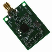
EVAL-ADF7021-NDBZ5 Analog Devices Inc, EVAL-ADF7021-NDBZ5 Datasheet
EVAL-ADF7021-NDBZ5
Specifications of EVAL-ADF7021-NDBZ5


Related parts for EVAL-ADF7021-NDBZ5


EVAL-ADF7021-NDBZ5 Summary of contents
Page 1
FEATURES Low power, narrow-band transceiver Frequency bands using dual VCO 80 MHz to 650 MHz 842 MHz to 916 MHz Programmable IF filter bandwidths of 9 kHz, 13.5 kHz, and 18.5 kHz Modulation schemes: 2FSK, 3FSK, 4FSK, MSK Spectral shaping: ...
Page 2
ADF7021-N TABLE OF CONTENTS Features .............................................................................................. 1 Applications....................................................................................... 1 Functional Block Diagram .............................................................. 1 Revision History ............................................................................... 2 General Description ......................................................................... 3 Specifications..................................................................................... 4 RF and PLL Specifications........................................................... 4 Transmission Specifications........................................................ 5 Receiver Specifications ................................................................ 6 Digital Specifications ................................................................... 9 ...
Page 3
GENERAL DESCRIPTION The ADF7021 high performance, low power, narrow- band transceiver based on the ADF7021. The ADF7021-N has IF filter bandwidths of 9 kHz, 13.5 kHz, and 18.5 kHz, making it ideally suited to worldwide narrowband standards and ...
Page 4
... ADF7021-N SPECIFICATIONS 3.6 V, GND = All measurements are performed with the EVAL-ADF7021-NDBxx using the PN9 data sequence, unless otherwise noted. RF AND PLL SPECIFICATIONS Table 1. Parameter RF CHARACTERISTICS Frequency Ranges (Direct Output) Frequency Ranges (RF Divide-by-2 Mode) Phase Frequency Detector (PFD) Frequency PHASE-LOCKED LOOP (PLL) ...
Page 5
TRANSMISSION SPECIFICATIONS Table 2. Parameter DATA RATE 2FSK, 3FSK 4FSK MODULATION 2 Frequency Deviation (f ) DEV Deviation Frequency Resolution Gaussian Filter BT Raised Cosine Filter Alpha TRANSMIT POWER 3 Maximum Transmit Power Transmit Power Variation vs. Temperature Transmit Power ...
Page 6
... For the definition of frequency deviation, refer to the Register 2—Transmit Modulation Register section. 3 Measured as maximum unmodulated power. 4 Conductive filtered harmonic emissions measured on the EVAL-ADF7021-NDBxx, which includes a T-stage harmonic filter (two inductors and one capacitor). 5 For matching details, refer to the LNA/PA Matching section. RECEIVER SPECIFICATIONS Table 3 ...
Page 7
Parameter Min 3FSK Sensitivity at 9.6 kbps Raised Cosine 3FSK Sensitivity at 9.6 kbps 4FSK Sensitivity at 9.6 kbps Raised Cosine 4FSK Sensitivity at 9.6 kbps INPUT IP3 Low Gain Enhanced Linearity Mode Medium Gain Mode High Sensitivity Mode ADJACENT ...
Page 8
... For received signal levels < −100 dBm recommended to average the RSSI readback value over a number of samples to improve the RSSI accuracy at low input powers. 3 Filtered conductive receive spurious emissions are measured on the EVAL-ADF7021-NDBxx, which includes a T-stage harmonic filter (two inductors and one capacitor). ...
Page 9
DIGITAL SPECIFICATIONS Table 4. Parameter Min TIMING INFORMATION Chip Enabled to Regulator Ready Chip Enabled to Tx Mode TCXO Reference XTAL Chip Enabled to Rx Mode TCXO Reference XTAL Tx-to-Rx Turnaround Time LOGIC INPUTS Input High Voltage, V 0.7 × ...
Page 10
... Low Current Mode High Sensitivity Mode POWER-DOWN CURRENT CONSUMPTION Low Power Sleep Mode 1 The transmit current consumption tests used the same combined PA and LNA matching network as that used on the EVAL-ADF7021-NDBxx evaluation boards. Improved PA efficiency is achieved by using a separate PA matching network. Min Typ Max ...
Page 11
TIMING CHARACTERISTICS ± 10%, DGND = AGND = Table 6. Parameter Limit MIN t > > > > >10 5 ...
Page 12
ADF7021-N TIMING DIAGRAMS Serial Interface SCLK t 1 SDATA DB31 (MSB) SLE SCLK SDATA REG7 DB0 (CONTROL BIT C1) SLE t 3 SREAD t 8 2FSK/3FSK Timing ±1 × DATA RATE/32 TxRxCLK TxRxDATA TxRxCLK TxRxDATA FETCH ...
Page 13
Timing In 4FSK receive mode, MSB/LSB synchronization should be guaranteed by SWD in the receive bit stream. t SYMBOL t BIT SLE TxRxCLK Rx SYMBOL TxRxDATA MSB Tx/Rx MODE SLE TxRxCLK Tx SYMBOL TxRxDATA MSB Tx/Rx MODE REGISTER 0 ...
Page 14
ADF7021-N UART/SPI Mode UART mode is enabled by setting R0_DB28 to 1. SPI mode is enabled by setting R0_DB28 to 1 and setting R15_DB[17:19] to 0x7. The transmit/receive data clock is available on the CLKOUT pin. CLKOUT (TRANSMIT/RECEIVE DATA CLOCK ...
Page 15
ABSOLUTE MAXIMUM RATINGS T = 25°C, unless otherwise noted. A Table 7. Parameter GND DD Analog I/O Voltage to GND Digital I/O Voltage to GND Operating Temperature Range Industrial (B Version) Storage Temperature Range Maximum Junction Temperature ...
Page 16
ADF7021-N PIN CONFIGURATION AND FUNCTION DESCRIPTIONS Table 8. Pin Function Descriptions Pin No. Mnemonic Description 1 VCOIN The tuning voltage on this pin determines the output frequency of the voltage controlled oscillator (VCO). The higher the tuning voltage, the higher ...
Page 17
Pin No. Mnemonic Description 29 GND2 Ground for Digital Section. 30 ADCIN Analog-to-Digital Converter Input. The internal 7-bit ADC can be accessed through this pin. Full scale 1.9 V. Readback is made using the SREAD pin. ...
Page 18
ADF7021-N TYPICAL PERFORMANCE CHARACTERISTICS –70 RF FREQ = 900MHz V –80 TEMPERATURE = 25°C VCO_BIAS = 8 VCO_ADJUST = 3 = 0.8mA – –100 –110 I = 2.2mA –120 CP –130 –140 –150 1 10 100 ...
Page 19
REF 15dBm ATTEN 25dB SAMP LOG 10dB 9.6kbps DATA = PRS9 f RF FREQ = 869.5MHz VAVG 100 3FSK RC3FSK CENTER 869.5MHz VBW 300Hz SWEEP2.226s (401pts) RES BW 300Hz Figure 17. Output Spectrum in ...
Page 20
ADF7021 FREQ = 868MHz 40 WANTED SIGNAL (10dB ABOVE SENSITIVITY 30 POINT) = 2FSK, f DEV 20 DATA RATE = 9.8kbps BLOCKER = 2FSK DEV DATA RATE = 9.8kbps ...
Page 21
RF I/P LEVEL = –70dBm 25kHz DATA RATE = 9.7kbps POST DEMOD BW = 12.4kHz f (inner) = 1.2kHz DEV 22452 ACQS M 50µs Figure 29. 4FSK Receiver Eye Diagram Measured Using ...
Page 22
ADF7021-N FREQUENCY SYNTHESIZER REFERENCE INPUT The on-board crystal oscillator circuitry (see Figure 32) can use a quartz crystal as the PLL reference. Using a quartz crystal with a frequency tolerance of ≤10 ppm for narrow-band applications is recommended ...
Page 23
... EVAL-ADF7021-NDBxx should be used for optimum performance. The free design tool ADI SRD Design Studio™ can also be used to design loop filters for the ADF7021-N (see the ADI SRD Design Studio web site for details). N Counter The feedback divider in the ADF7021-N PLL consists of an 8-bit integer counter (R0_DB[19:26]) and a 15-bit, sigma-delta (Σ ...
Page 24
ADF7021-N VOLTAGE CONTROLLED OSCILLATOR (VCO) The ADF7021-N contains two VCO cores. The first VCO, the internal inductor VCO, uses an internal LC tank and supports 842 MHz to 916 MHz and 421 MHz to 458 MHz operating bands. The second ...
Page 25
Table 9. RF Output Frequency Ranges for Internal and External Inductor VCOs and Required Register Settings RF Frequency VCO to RF Divide Output (MHz) Be Used by 2 870 to 916 Internal L No 842 to 870 Internal L No ...
Page 26
ADF7021-N TRANSMITTER RF OUTPUT STAGE The power amplifier (PA) of the ADF7021-N is based on a single-ended, controlled current, open-drain amplifier that has been designed to deliver dBm into a 50 Ω load at a maximum frequency ...
Page 27
Setting the Transmit Data Rate In all modulation modes except oversampled 2FSK mode, an accurate clock is provided on the TxRxCLK pin to latch the data from the microcontroller into the transmit section at the required data rate. The exact ...
Page 28
ADF7021-N The signal mapping of the input binary transmit data to the 3-level convolutional output is shown in Table 10. The convolutional encoder restricts the maximum number of sequential +1s or −1s to two and delivers an equal number of ...
Page 29
MODULATION AND FILTERING OPTIONS The various modulation and data filtering options are described in Table 11. Table 11. Modulation and Filtering Options Modulation Data Filtering BINARY FSK 2FSK None 1 MSK None OQPSK with Half Sine None 2 Baseband Shaping ...
Page 30
ADF7021-N RECEIVER SECTION RF FRONT END The ADF7021-N is based on a fully integrated, low IF receiver architecture. The low IF architecture facilitates a very low external component count and does not suffer from powerline- induced interference problems. Figure 45 ...
Page 31
The user has the option of changing the two threshold values from the defaults of 30 and 70 (Register 9). The default AGC setup values should be adequate for most applications. The threshold values must be more than 30 apart ...
Page 32
ADF7021-N DEMODULATION, DETECTION, AND CDR System Overview An overview of the demodulation, detection, and clock and data recovery (CDR) of the received signal on the ADF7021-N is shown in Figure 47. The quadrature outputs of the IF filter are first ...
Page 33
Linear Demodulator Figure 49 shows a block diagram of the linear demodulator. I LEVEL IF LIMITER Q FREQUENCY LINEAR DISCRIMINATOR R4_DB(20:29) Figure 49. Block Diagram of Linear FSK Demodulator A digital frequency discriminator provides an output signal that is linearly ...
Page 34
ADF7021-N For example, using 2FSK with Manchester-encoded data achieves a data rate tolerance of ±2.0%. The CDR PLL is designed for fast acquisition of the recovered symbols during preamble and typically achieves bit synchro- nization within 5-symbol transitions of preamble. ...
Page 35
Viterbi Detector Setup The Viterbi detector can be used for 3FSK data detection. This is activated by setting R13_DB11 to Logic 1. The Viterbi path memory length is programmable in steps bits (VITERBI_PATH_MEMORY, ...
Page 36
ADF7021-N DEMODULATOR CONSIDERATIONS 2FSK Preamble The recommended preamble bit pattern for 2FSK is a dc-free pattern (such as a 10101010… pattern). Preamble patterns with longer run-length constraints (such as 11001100…) can also be used but result in a longer synchronization ...
Page 37
Internal AFC The ADF7021-N supports a real-time, internal, automatic frequency control loop. In this mode, an internal control loop automatically monitors the frequency error and adjusts the synthesizer-N divider using an internal proportional integral (PI) control loop. The internal AFC ...
Page 38
ADF7021-N APPLICATIONS INFORMATION IF FILTER BANDWIDTH CALIBRATION The IF filter should be calibrated on every power-up in receive mode to correct for errors in the bandwidth and filter center frequency due to process variations. The automatic calibration requires no external ...
Page 39
... Internal Rx/Tx Switch Figure 50 shows the ADF7021 configuration where the internal Rx/Tx switch is used with a combined LNA/PA matching network. This is the configuration used on the EVAL- ADF7021-NDBxx evaluation board. For most applications, the slight performance degradation caused by the internal Rx/Tx switch is acceptable, allowing the user to take advantage of the cost saving potential of this solution ...
Page 40
ADF7021-N External Rx/Tx Switch Figure 51 shows a configuration using an external Rx/Tx switch. This configuration allows an independent optimization of the matching and filter network in the transmit and receive path. Therefore more flexible and less difficult ...
Page 41
RFIN LNA RFINB INTERNAL SOURCE Figure 52. Image Rejection Calibration Using the Internal Calibration Source and a Microcontroller Using the internal RF source, the RF frequencies that can be used for image calibration are programmable and are odd multiples of ...
Page 42
ADF7021-N PACKET STRUCTURE AND CODING The suggested packet structure to use with the ADF7021-N is shown in Figure 54. SYNC ID PREAMBLE WORD FIELD DATA FIELD Figure 54. Typical Format of a Transmit Protocol Refer to the Receiver Setup section ...
Page 43
TCXO REFERENCE CE HIGH WAIT 10µs (REGULATOR POWER-UP) WRITE TO REGISTER 1 (TURNS ON VCO) WAIT 0.7ms (TYPICAL VCO SETTLING) WRITE TO REGISTER 3 (TURNS ON Tx/Rx CLOCKS) WRITE TO REGISTER 0 (TURNS ON PLL) WAIT 40µs (TYPICAL PLL SETTLING) ...
Page 44
ADF7021-N REFERENCE CE HIGH WAIT 10µs (REGULATOR POWER-UP) OPTIONAL. TCXO POWER-DOWN CE LOW WRITE TO REGISTER 1 (TURNS ON VCO) WAIT 0.7ms (TYPICAL VCO SETTLING) WRITE TO REGISTER 3 (TURNS ON Tx/Rx CLOCKS) WRITE TO REGISTER 6 (SETS UP IF ...
Page 45
... Figure 57. Typical Application Circuit (Regulator Capacitors and Power Supply Decoupling Not Shown) For recommended component values, refer to the ADF7021-N evaluation board data sheet and AN-859 application note accessible from the ADF7021-N product page. Follow the reference design schematic closely to ensure optimum performance in narrow-band applications ...
Page 46
ADF7021-N SERIAL INTERFACE The serial interface allows the user to program the 16-/32-bit registers using a 3-wire interface (SCLK, SDATA, and SLE). It consists of a level shifter, 32-bit shift register, and 16 latches. Signals should be CMOS compatible. The ...
Page 47
Battery Voltage/ADCIN/Temperature Sensor Readback The battery voltage is measured at Pin VDD4. The readback information is contained in Bit RV1 to Bit RV7. This also applies to the readback of the voltage at the ADCIN pin and the temperature sensor. ...
Page 48
ADF7021-N INTERFACING TO A MICROCONTROLLER/DSP Standard Transmit/Receive Data Interface The standard transmit/receive signal and configuration interface to a microcontroller is shown in Figure 59. In transmit mode, the ADF7021-N provides the data clock on the TxRxCLK pin, and the TxRxDATA ...
Page 49
REGISTER 0—N REGISTER MUXOUT INTEGER_N TR1 Tx/Rx 0 TRANSMIT 1 RECEIVE U1 UART_MODE 0 DISABLED 1 ENABLED MUXOUT REGULATOR_READY (DEFAULT FILTER_CAL_COMPLETE DIGITAL_LOCK_DETECT RSSI_READY 1 0 ...
Page 50
ADF7021-N REGISTER 1—VCO/OSCILLATOR REGISTER VCO CENTER VA2 VA1 FREQ ADJUST 0 0 NOMINAL 0 1 VCO ADJUST VCO ADJUST VCO ADJUST UP 3 VB4 VB3 VB2 VB1 ...
Page 51
REGISTER 2—TRANSMIT MODULATION REGISTER TxDATA_ INVERT Tx_FREQUENCY_DEVIATION DI2 DI1 TxDATA_INVERT 0 0 NORMAL 0 1 INVERT CLK 1 0 INVERT DATA 1 1 INV CLK AND DATA TFD9 ... TFD3 TFD2 0 ... 0 0 ... ...
Page 52
ADF7021-N REGISTER 3—TRANSMIT/RECEIVE CLOCK REGISTER AGC_CLK_DIVIDE SEQ_CLK_DIVIDE GD4 GD3 GD2 GD1 GD6 GD5 ... ... ... ... ... ... • Baseband offset ...
Page 53
REGISTER 4—DEMODULATOR SETUP REGISTER POST_DEMOD_BW IF_FILTER _ IFB2 IFB1 kHz 0 1 13.5 kHz 1 0 18.5 kHz 1 1 INVALID POST_DEMOD_ DW10 . DW6 DW5 DW4 DW3 DW2 DW1 ...
Page 54
ADF7021-N REGISTER 5—IF FILTER SETUP REGISTER IR_GAIN_ ADJUST_MAG PM3 PD1 IR_PHASE_ADJUST_DIRECTION 0 ADJUST ADJUST Q CH GM5 GM4 GM3 GM2 GM1 ...
Page 55
REGISTER 6—IF FINE CAL SETUP REGISTER IF_CAL_DWELL_TIME IRD1 IR_CAL_SOURCE ÷2 0 SOURCE ÷2 OFF SOURCE ÷ IR_CAL_SOURCE_ IRC2 IRC1 DRIVE_LEVEL 0 0 OFF 0 1 LOW 1 0 MED 1 1 HIGH CD3 CD7 ... 0 0 ... ...
Page 56
ADF7021-N REGISTER 7—READBACK SETUP REGISTER RB3 READBACK_SELECT 0 DISABLED 1 ENABLED • Readback of the measured RSSI value is valid only in Rx mode. Readback of the battery voltage, temperature sensor, or voltage at the external pin is not valid ...
Page 57
REGISTER 8—POWER-DOWN TEST REGISTER Rx_RESET DB15 DB14 CR1 CR1 COUNTER_RESET 0 NORMAL 1 RESET CDR RESET PD7 PA (Rx MODE OFF SW1 0 1 LE1 LOG_AMP_ENABLE 0 LOG AMP OFF 1 LOG AMP ON • ...
Page 58
ADF7021-N REGISTER 9—AGC REGISTER ML1 MIXER_LINEARITY 0 DEFAULT 1 HIGH LI2 LI1 LNA_BIAS 0 0 800µA (DEFAULT) LG1 LNA_MODE 0 DEFAULT 1 REDUCED GAIN FI1 FILTER_CURRENT 0 LOW 1 HIGH FG2 FG1 FILTER_GAIN ...
Page 59
REGISTER 10—AFC REGISTER MAX_AFC_RANGE KP3 KP2 KP1 MAX_AFC_ ... MA3 MA2 MA1 MA8 RANGE 0 ... ... ... ...
Page 60
ADF7021-N REGISTER 11—SYNC WORD DETECT REGISTER REGISTER 12—SWD/THRESHOLD SETUP REGISTER SWD_MODE 0 SWD PIN LOW 1 SWD PIN HIGH AFTER NEXT SYNCWORD 2 SWD PIN HIGH AFTER NEXT SYNCWORD FOR DATA PACKET LENGTH NUMBER OF BYTES 3 INTERRUPT PIN HIGH ...
Page 61
REGISTER 13—3FSK/4FSK DEMOD REGISTER Refer to the Receiver Setup section for information about programming these settings. 3FSK_PREAMBLE_ TIME_VALIDATE 3FSK_CDR_THRESHOLD VT7 ... VT3 0 0 ... 0 0 ... 0 0 ... 0 0 ... . . ... . ... . ...
Page 62
ADF7021-N REGISTER 14—TEST DAC REGISTER TEST_DAC_GAIN ED_LEAK_FACTOR PULSE_EXTENSION LEAKAGE = 0 0 2^– 2^– 2^– 2^–11 4 2^–12 5 2^–13 6 2^–14 7 2^–15 ED_PEAK_RESPONSE 0 FULL RESPONSE TO PEAK 1 0.5 RESPONSE TO ...
Page 63
REGISTER 15—TEST MODE REGISTER ANALOG_TEST_ MODES CAL_OVERRIDE 0 AUTO CAL 1 OVERRIDE GAIN 2 OVERRIDE BW 3 OVERRIDE BW AND GAIN REG1_PD 0 NORMAL 1 PWR DWN FORCE_LD_HIGH 0 NORMAL 1 FORCE ANALOG_TEST_MODES 0 BAND GAP VOLTGE 1 40µA CURRENT ...
Page 64
... ADF7021-NDF −40°C to +85°C 1 EVAL-ADF70XXMBZ2 1 EVAL-ADF7021-NDBIZ 1 EVAL-ADF7021-NDBEZ 1 EVAL-ADF7021-NDBZ2 1 EVAL-ADF7021-NDBZ5 RoHS Compliant Part. ©2008 Analog Devices, Inc. All rights reserved. Trademarks and registered trademarks are the property of their respective owners. 7.00 BSC SQ 0.60 MAX 36 TOP 6.75 VIEW BSC SQ 0 ...