KSZ8841-16MBL Micrel Inc, KSZ8841-16MBL Datasheet
KSZ8841-16MBL
Specifications of KSZ8841-16MBL
Available stocks


Related parts for KSZ8841-16MBL


KSZ8841-16MBL Summary of contents
Page 1
... Ethernet MAC controller, an 8-bit, 16-bit, and 32-bit generic host processor interface and incorporates a unique dynamic memory pointer with 4-byte buffer boundary and a fully utilizable 8KB for both TX and RX directions in host buffer interface. The KSZ8841M is designed to be fully compliant with the appropriate IEEE 802.3 standards. ...
Page 2
... RX/TX FIFO buffers • Early TX/RX functions to minimize latency through the device • Optional to use external serial EEPROM configuration for both KSZ8841-16MQL and KSZ8841-32MQL • Single 25MHz reference clock for both PHY and MAC Network Features • Fully integrated to comply with IEEE802.3u standards • ...
Page 3
... Updated Figure 12/13/14 Asynchronous Timing and Table 16/17/18 parameters, PQFP package information. Added QMU RX Flow Control High Watermark QRFCR register and updated body text Improve the ARDY low time in read cycle and in write cycle during QMU data register access Add KSZ8841-16MBL 100-Ball BGA package information 3 KSZ8841-16/32 MQL/MVL/MBL Package 128-Pin PQFP ...
Page 4
... Pin Configuration for KSZ8841-16 Chip (8/16-Bit) ........................................................................................................... 10 Ball Configuration for KSZ8841-16 Chip (8/16-Bit) .......................................................................................................... 11 Pin Description for KSZ8841-16 Chip (8/16-Bit) ............................................................................................................... 12 Ball Description for KSZ8841-16 Chip (8/16-Bit) .............................................................................................................. 17 Pin Configuration for KSZ8841-32 Chip (32-Bit) .............................................................................................................. 21 Pin Description for KSZ8841-32 Chip (32-Bit) .................................................................................................................. 22 Functional Description ....................................................................................................................................................... 27 Functional Overview ........................................................................................................................................................... 27 Power Management ..................................................................................................................................................... 27 Power down ...
Page 5
... Bank 7 Wakeup Frame 3 Byte Mask 3 Register (0x0A): WF3BM3.............................................................................. 62 Bank 8 – 15: Reserved ................................................................................................................................................. 62 Bank 16 Transmit Control Register (0x00): TXCR ....................................................................................................... 63 Bank 16 Transmit Status Register (0x02): TXSR......................................................................................................... 63 Bank 16 Receive Control Register (0x04): RXCR........................................................................................................ 64 Bank 16 TXQ Memory Information Register (0x08): TXMIR........................................................................................ 64 October 2007 KSZ8841-16/32 MQL/MVL/MBL 5 M9999-102207-1.6 ...
Page 6
... MIB (Management Information Base) Counters............................................................................................................... 85 Additional MIB Information ........................................................................................................................................... 86 (1) Absolute Maximum Ratings ............................................................................................................................................ 87 (1) Operating Ratings ............................................................................................................................................................ 87 (1) Electrical Characteristics ................................................................................................................................................ 88 Timing Specifications ......................................................................................................................................................... 89 Asynchronous Timing without using Address Strobe (ADSN = 0) ............................................................................... 89 Asynchronous Timing using Address Strobe (ADSN) .................................................................................................. 90 Asynchronous Timing using DATACSN ....................................................................................................................... 91 October 2007 KSZ8841-16/32 MQL/MVL/MBL 6 M9999-102207-1.6 ...
Page 7
... Synchronous Timing in Burst Read (VLBUSN = 1) .................................................................................................................... 94 Synchronous Write Timing (VLBUSN = 0) ................................................................................................................................. 95 Synchronous Read Timing (VLBUSN = 0) ................................................................................................................................. 96 Auto Negotiation Timing............................................................................................................................................................. 97 Reset Timing.............................................................................................................................................................................. 98 EEPROM Timing........................................................................................................................................................................ 99 Selection of Isolation Transformers................................................................................................................................ 100 Selection of Reference Crystal ........................................................................................................................................ 100 Package Information ......................................................................................................................................................... 101 Acronyms and Glossary................................................................................................................................................... 104 October 2007 KSZ8841-16/32 MQL/MVL/MBL 7 M9999-102207-1.6 ...
Page 8
... List of Figures Figure 1. KSZ8841M Functional Diagram............................................................................................................................... 1 Figure 2. Standard – KSZ8841-16MQL 128-Pin PQFP ........................................................................................................ 10 Figure 3. Option – KSZ8841-16MVL 128-Pin LQFP............................................................................................................. 10 Figure 4. KSZ8841-16MBL 100-Ball LFBGA (Top View)...................................................................................................... 11 Figure 5. Standard – KSZ8841-32MQL 128-Pin PQFP ........................................................................................................ 21 Figure 6. Option – KSZ8841-32MVL 128-Pin LQFP............................................................................................................. 21 Figure 7. Typical Straight Cable Connection ........................................................................................................................ 30 Figure 8 ...
Page 9
... Table 5. Transmit Byte Count Format................................................................................................................................... 39 Table 6. Frame Format for Receive Queue .......................................................................................................................... 39 Table 7. RXQ Receive Packet Status Word ......................................................................................................................... 40 Table 8. RXQ Receive Packet Byte Count Word.................................................................................................................. 40 Table 9. KSZ8841M EEPROM Format ................................................................................................................................. 40 Table 10. ConfigParam Word in EEPROM Format............................................................................................................... 41 Table 11. Format of MIB Counters........................................................................................................................................ 85 Table 12. Port 1 MIB Counters Indirect Memory Offsets ...................................................................................................... 86 Table 13 ...
Page 10
... KSZ8841-16 NC 106 107 108 109 NC 110 D15 MVL 111 D14 112 D13 113 D12 114 D11 115 D10 D9 116 D8 117 D7 118 D6 119 (Top View) D5 120 D4 121 D3 122 123 124 125 D2 126 D1 127 D0 128 Figure 3. Option – KSZ8841-16MVL 128-Pin LQFP 10 KSZ8841-16/32 MQL/MVL/MBL ...
Page 11
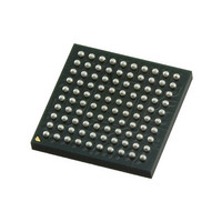
... Micrel, Inc. Ball Configuration for KSZ8841-16 Chip (8/16-Bit) October 2007 Figure 4. KSZ8841-16MBL 100-Ball LFBGA (Top View) 11 KSZ8841-16/32 MQL/MVL/MBL M9999-102207-1.6 ...
Page 12
... Local bus clock for synchronous bus systems. Maximum frequency is 50MHz. This pin should be tied Low or unconnected asynchronous mode. No Connect. Power Management Event Not When asserted (Low), this signal indicates that a power management event has occurred in the system when a wake-up signal is detected by KSZ8841M. 12 KSZ8841-16/32 MQL/MVL/MBL [0,1] — ...
Page 13
... For VLBus-like mode, the falling edge of this signal indicates ready. This signal is synchronous to the bus clock signal BCLK. For burst mode (32-bit interface only), the KSZ8841M drives this pin low to signal wait states. Interrupt Active Low signal to host CPU to indicate an interrupt status bit is set, this pin need an external 4 ...
Page 14
... No Connect No Connect Analog ground No Connect No Connect 1.2 analog V input power supply from VDDCO (pin24) through external Ferrite bead and DD capacitor. Analog ground No connect No connect Set physical transmits output current. Pull-down this pin with a 3.01K 1% resistor to ground. Analog ground 14 KSZ8841-16/32 MQL/MVL/MBL M9999-102207-1.6 ...
Page 15
... Digital core ground 1.2V digital core V input power supply from VDDCO (pin24) through external Ferrite DD bead and capacitor. 3.3V digital V input power supply for IO with well decoupling capacitors. DDIO No Connect No Connect No Connect No Connect No Connect No Connect No Connect No Connect No Connect No Connect 15 KSZ8841-16/32 MQL/MVL/MBL M9999-102207-1.6 ...
Page 16
... IO with well decoupling capacitors. DDIO No Connect Data 15 Data 14 Data 13 Data 12 Data 11 Data 10 Data 9 Data 8 Data 7 Data 6 Data 5 Data 4 Data 3 Digital IO ground Digital core ground 3.3V digital V input power supply for IO with well decoupling capacitors. DDIO Data 2 Data 1 Data 0 16 KSZ8841-16/32 MQL/MVL/MBL M9999-102207-1.6 ...
Page 17
... This ball should be tied Low or unconnected asynchronous mode. Power Management Event Not When asserted (Low), this signal indicates that a power management event has occurred in the system when a wake-up signal is detected by KSZ8841M. Synchronous Ready Not Ready signal to interface with synchronous bus for both EISA-like and VLBus- like extend accesses ...
Page 18
... October 2007 Ball Function Active Low output signal, asserted when AEN is Low and A15-A4 decode to the KSZ8841M address programmed into the high byte of the base address register. LDEVN is a combinational decode of the Address and AEN signal. Read Strobe Not Asynchronous read strobe, active Low. ...
Page 19
... Byte Enable 1 Not, Active low for Data byte 1 enable (don’t care in 8-bit bus mode). I Byte Enable 0 Not, Active low for Data byte 0 enable (there is an internal inverter enabled and connected to the BE1N for 8-bit bus mode). Data 15 Data 14 Data 13 Data 12 Data 11 Data 10 Data 9 Data 8 Data 7 Data 6 Data 5 Data 4 Data 3 19 KSZ8841-16/32 MQL/MVL/MBL M9999-102207-1.6 ...
Page 20
... Ferrite bead and capacitor. P 3.3V analog V input power supply with well decoupling capacitors 3.3V analog V input power supply with well decoupling capacitors 3.3V digital V input power supply for IO with well decoupling capacitors. DDIO All digital and analog grounds No Connect 20 KSZ8841-16/32 MQL/MVL/MBL M9999-102207-1.6 ...
Page 21
... KSZ8841-32 108 109 D16 110 D15 111 D14 MVL 112 D13 113 D12 114 D11 D10 115 D9 116 D8 117 D7 118 (Top View) D6 119 D5 120 D4 121 D3 122 123 124 125 D2 126 D1 127 D0 128 Figure 6. Option – KSZ8841-32MVL 128-Pin LQFP 21 KSZ8841-16/32 MQL/MVL/MBL ...
Page 22
... When DATACSN is Low, the data path can be accessed regardless of the value of AEN, A15-A1, and the content of the BANK select register. Power Management Event Not When asserted (Low), this signal indicates that a power management event has occurred in the system when a wake-up signal is detected by KSZ8841M. 22 KSZ8841-16/32 MQL/MVL/MBL [0,1] — ...
Page 23
... For VLBus-like mode, the falling edge of this signal indicates ready. This signal is synchronous to the bus clock signal BCLK. For burst mode (32-bit interface only), the KSZ8841M drives this pin low to signal wait states. Interrupt Active Low signal to host CPU to indicate an interrupt status bit is set, this pin need an external 4 ...
Page 24
... No Connect No Connect Analog ground No Connect No Connect 1.2 analog V input power supply from VDDCO (pin24) through external Ferrite bead and DD capacitor. Analog ground No connect No connect Set physical transmits output current. Pull-down this pin with a 3.01K 1% resistor to ground. Analog ground 24 KSZ8841-16/32 MQL/MVL/MBL M9999-102207-1.6 ...
Page 25
... Digital core ground 1.2V digital core V input power supply from VDDCO (pin24) through external Ferrite DD bead and capacitor. 3.3V digital V input power supply for IO with well decoupling capacitors. DDIO Data 30 Data 29 Data 28 Data 27 Data 26 Data 25 Data 24 Data 23 Data 22 Data 21 25 KSZ8841-16/32 MQL/MVL/MBL M9999-102207-1.6 ...
Page 26
... IO with well decoupling capacitors. DDIO Data 16 Data 15 Data 14 Data 13 Data 12 Data 11 Data 10 Data 9 Data 8 Data 7 Data 6 Data 5 Data 4 Data 3 Digital IO ground Digital core ground 3.3V digital V input power supply for IO with well decoupling capacitors. DDIO Data 2 Data 1 Data 0 26 KSZ8841-16/32 MQL/MVL/MBL M9999-102207-1.6 ...
Page 27
... Power Management Power down The KSZ8841M features a port power-down mode. To save power, the user can power-down the port that is not in use by setting bit 11 in either P1CR4 or P1MBCR register for this port. To bring the port back up, reset bit 11 in these registers. In addition, there is a full chip power-down mode PWRDN (pin 36). When this pin is pulled-down, the entire chip powers down ...
Page 28
... If the LAN controller scans a frame and does not find the specific sequence shown above, it discards the frame and takes no further action. If the KSZ8841M controller detects the data sequence, however, it then alerts the PC’s power management circuitry (assert the PMEN pin) to wake up the system. ...
Page 29
... The auto-sense function detects remote transmit and receive pairs and correctly assigns the transmit and receive pairs for the KSZ8841M device. This feature is extremely useful when end users are unaware of cable types in addition to saving on an additional uplink configuration connection. The auto-crossover feature can be disabled through the port control registers ...
Page 30
... Figure 7. Typical Straight Cable Connection 10/100 Ethernet Media Dependent Interface 1 Crossover Receive Pair Cable Transmit Pair Modular Connector (RJ-45) HUB (Repeater or Switch) Figure 8. Typical Crossover Cable Connection 30 KSZ8841-16/32 MQL/MVL/MBL MDI-X Signals 1 RD+ 2 RD- 3 TD itc ) h 10/100 Ethernet Media Dependent Interface ...
Page 31
... If auto negotiation is not supported or the link partner to the KSZ8841M is forced to bypass auto negotiation, the mode is set by observing the signal at the receiver. This is known as parallel mode because while the transmitter is sending auto negotiation advertisements, the receiver is listening for advertisements or a fixed signal protocol ...
Page 32
... If P1VCT[14:13]=11, this indicates an invalid test, and occurs when the KSZ8841M is unable to shut down the link partner. In this instance, the test is not run not possible for the KSZ8841M to determine if the detected signal is a reflection of the signal generated or a signal from another source. ...
Page 33
... Half-Duplex Backpressure A half-duplex backpressure option (non-IEEE 802.3 standards) is also provided. The activation and deactivation conditions are the same as in full-duplex mode. If backpressure is required, the KSZ8841M sends preambles to defer the other stations' transmission (carrier sense deference). To avoid jabber and excessive deference (as defined in the 802.3 standard), after a certain time, the KSZ8841M discontinues the carrier sense and then raises it again quickly ...
Page 34
... Note 1: BE3N, BE2N, BE1N and BE0N are ignored when DATACSN is low because 32 bit transfers are assumed. Note 2: BE2N and BE3N are valid only for the KSZ8841-32 mode, and are No Connect for the KSZ8841-16 mode. Data For KSZ8841M-32 mode only. Data ...
Page 35
... ADSN to latch the address on the rising edge. The BIU decodes latched A[15:4] and qualifies with AEN to determine if the KSZ8841M device is the intended target. The data transfer is the same as the first case. Interfacing with the system/host relying on central decoding (KSZ8841-32MQL only). ...
Page 36
... This interface is used in an architecture in which the device’s local decoder is utilized; that is, the BIU decodes latched A[15:4] and qualifies with AEN (Address Enable) to determine if the KSZ8841M device is the intended target. No burst is supported in this application. The M/nIO signal connection in VLBus is routed to AEN. The CYCLEN in this application is used to sample the SWR signal when it is asserted ...
Page 37
... Figure 11. KSZ8841M 8-Bit, 16-Bit, and 32-Bit Data Bus Connections BIU Implementation Principles Since KSZ8841M is an I/O device with 16 addressable locations, address decoding is based on the values of A15-A4 and AEN. Whenever DATACSN is asserted, the address decoder is disabled and a 32-bit transfer to Data Register is assumed (BE3N – BE0N are ignored). ...
Page 38
... The EISA-like burst transfer is supported using synchronous interface signals and DATACSN when I/O signal VLBUSN = 1. Both the system/host/memory and KSZ8841M are capable of inserting wait states. To set the system/host/memory to insert a wait state, assert RDYRTNN signal. To set the KSZ8841M to insert a wait state, assert SRDYN signal. Queue Management Unit (QMU) The Queue Management Unit (QMU) manages packet traffic between the MAC/PHY interface and the system host ...
Page 39
... The data area contains six bytes of Destination Address (DA) followed by six bytes of Source Address (SA), followed by a variable-length number of bytes. On transmit, all bytes are provided by the CPU, including the source address. The KSZ8841M does not insert its own SA. The 802.3 Frame Length word (Frame Type in Ethernet) is not interpreted by the KSZ8841M treated transparently as data both for transmit operations. ...
Page 40
... Receive Byte Count up to 1916 bytes EEPROM Interface It is optional in the KSZ8841M to use an external EEPROM. In the case that an EEPROM is not used, the EEEN pin must be tied Low or floating. An external serial EEPROM with a standard microwire bus interface is used for non-volatile storage of information such as the host MAC address, base address, and default configuration settings ...
Page 41
... D2 Support When this bit is set, the KSZ8841M supports D2 power state. This bit is loaded to bit 10 of PMCR register. D1 Support When this bit is set, the KSZ8841M supports D1 power state. This bit is loaded to bit 9 of PMCR register. Reserved. Internal clock rate selection 0: 125 MHz 1: 25 MHz Note: At power up, this chip operates on 125 MHz clock ...
Page 42
... PHY port will be set to 100BASE-TX full-duplex mode. Near-end (Remote) Loopback Near-end (Remote) loopback is conducted at PHY port 1of the KSZ8841M. The loopback path starts at the PHY port’s receive inputs (RXP1/RXM1), wraps around at the same PHY port’s PMD/PMA, and ends at the PHY port’s transmit outputs (TXP1/TXM1) ...
Page 43
... Micrel, Inc. CPU Interface I/O Registers The KSZ8841M provides an EISA-like, ISA-like, or VLBUS-like bus interface for the CPU to access its internal I/O registers. I/O registers serve as the address that the microprocessor uses when communicating with the device. This is used for configuring operational settings, reading or writing control, status information, and transferring packets by reading and writing through the packet data registers ...
Page 44
... Reserved Power Management Capabilities [15:8] Wakeup Frame Control [7:0] Reserved Wakeup Frame Control [15:8] Reserved Bank Select [7:0] Bank Select [15:8] 44 KSZ8841-16/32 MQL/MVL/MBL Bank 4 Bank 5 Bank 6 Wakeup Wakeup Wakeup Frame0 Frame1 Frame2 CRC0 [7:0] CRC0 [7:0] CRC0 [7:0] Wakeup Wakeup Wakeup ...
Page 45
... To 0xE 0xF 0xE - 0xF 0xF October 2007 Bank Location Bank 9 Bank 10 Bank 11 Reserved Reserved Reserved Reserved Reserved Reserved Reserved Bank Select [7:0] Bank Select [15:8] 45 KSZ8841-16/32 MQL/MVL/MBL Bank 12 Bank 13 Bank 14 M9999-102207-1.6 Bank 15 ...
Page 46
... Low Transmit Management Control/Status [15:8] [15:8] [15:8] QMU Data Early High Receive [7:0] [7:0] QMU Data Early High Receive [15:8] [15:8] Reserved Bank Select [7:0] Bank Select [15:8] 46 KSZ8841-16/32 MQL/MVL/MBL Bank 20 Bank 21 Bank 22 Reserved Reserved Reserved Reserved Reserved Reserved M9999-102207-1.6 Bank 23 ...
Page 47
... To 0xE 0xF 0xE - 0xF 0xF October 2007 Bank Location Bank 25 Bank 26 Bank 27 Reserved Reserved Reserved Reserved Reserved Reserved Reserved Bank Select [7:0] Bank Select [15:8] 47 KSZ8841-16/32 MQL/MVL/MBL Bank 28 Bank 29 Bank 30 M9999-102207-1.6 Bank 31 ...
Page 48
... Chip Global Control 0xB [15:8] 0xC 0xC - 0xD 0xD 0xC To 0xE 0xF 0xE - 0xF 0xF October 2007 Bank Location Bank 33 Bank 34 Bank 35 Reserved Reserved Reserved Reserved Reserved Bank Select [7:0] Bank Select [15:8] 48 KSZ8841-16/32 MQL/MVL/MBL Bank 36 Bank 37 Bank 38 Reserved Reserved M9999-102207-1.6 Bank 39 ...
Page 49
... Data 4 [7:0] Reserved Indirect Access Data 4 [15:8] Indirect Access Data 5 [7:0] Reserved Indirect Access Data 5 [15:8] Bank Select [7:0] Bank Select [15:8] 49 KSZ8841-16/32 MQL/MVL/MBL Bank 44 Bank 45 Bank 46 PHY1 MII- Register Basic Control [7:0] Reserved PHY1 MII- Register Basic Control [15:8] PHY1 MII- ...
Page 50
... Control/Status, LinkMD [7:0] Port 1 PHY Special Control/Status, LinkMD [15:8] Port 1 Control 4 [7:0] Port 1 Control 4 [15:8] Port 1 Status [7:0] Port 1 Status [15:8] Reserved Reserved Reserved Reserved Bank Select [7:0] Bank Select [15:8] 50 KSZ8841-16/32 MQL/MVL/MBL Bank 52 Bank 53 Bank 54 Reserved Reserved Reserved M9999-102207-1.6 Bank 55 ...
Page 51
... To 0xE 0xF 0xE - 0xF 0xF October 2007 Bank Location Bank 57 Bank 58 Bank 59 Reserved Reserved Reserved Reserved Reserved Reserved Reserved Bank Select [7:0] Bank Select [15:8] 51 KSZ8841-16/32 MQL/MVL/MBL Bank 60 Bank 61 Bank 62 M9999-102207-1.6 Bank 63 ...
Page 52
... Description BARH Base Address High These bits are compared against the address on the bus ADDR[15:8] to determine the BASE for the KSZ8841M registers. BARL Base Address Low These bits are compared against the address on the bus ADDR[7:5] to determine the BASE for the KSZ8841M registers. ...
Page 53
... Synchronous and Asnychronous Transfers occur simultaneously. 0: normal. Write 1 to clear. Reserved. Description Reserved. BRL Burst Length (for burst read and write) 000: single. 011: fixed burst read length of 4. 101: fixed burst read length of 8. 111: fixed burst read length of 16. Reserved. 53 KSZ8841-16/32 MQL/MVL/MBL M9999-102207-1.6 ...
Page 54
... MARM[15:0] = EEPROM 0x2(MAC Byte 4 and 3) MARH[15:0] = EEPROM 0x3(MAC Byte 6 and 5) The Host MAC address is used to define the individual destination address that the KSZ8841M responds to when receiving frames. Network addresses are generally expressed in the form of 01:23:45:67:89:AB, where the bytes are received from left to right, and the bits within each byte are received from right to left (LSB to MSB). For example, the actual transmitted and received bits are on the order of 10000000 11000100 10100010 11100110 10010001 11010101 ...
Page 55
... Bank 3 On-Chip Bus Control Register (0x00): OBCR This register controls the on-chip bus speed for the KSZ8841M used for power management when the external host CPU is running at a slow frequency. The default of the on-chip bus speed is 125 MHz without EEPROM. When the external host CPU is running at a higher clock rate, the on-chip bus should be adjusted for the best performance ...
Page 56
... PME Support D3 (cold) This bit defaults the KSZ8841M does not support D3(cold) PME Support D3 (hot) This bit is 1 only,it is indicating that the KSZ8841M can assert PME event (PMEN pin 14) in D3(hot) power state.(see bit1:0 in PMCS register) PME Support D2 If this bit is set, the wake-up signals will assert PME event (PMEN pin 14) when the KSZ8841M power state and PME_EN (see bit8 in PMCS register) is set ...
Page 57
... October 2007 Description (PMEN pin 14 power state. D2 Support If this bit is set, it indicates that the KSZ8841M support D2 power state. The value of this bit is loaded from the D2_SUP bit of 0x6 in the serial EEPROM (without an EEPROM, this bit defaults to 0). D1 Support If this bit is set, it indicates that the KSZ8841M support D1 power state. The value of this bit is loaded from the D1_SUP bit of 0x6 in the serial EEPROM (without an EEPROM, this bit defaults to 0) ...
Page 58
... The first 16 bytes mask of a Wake up frame 0 pattern. Description WF0BM1 Wake up Frame 0 Byte Mask 1. The next 16 bytes mask covering bytes Wake up frame 0 pattern. Description WF0BM2 Wake-up Frame 0 Byte Mask 2. The next 16 bytes mask covering bytes Wake-up frame 0 pattern. 58 KSZ8841-16/32 MQL/MVL/MBL M9999-102207-1.6 ...
Page 59
... Wake-up frame 1 CRC (upper 16 bits). The expected CRC value of a Wake-up frame 1 pattern. Description WF1BM0 Wake-up frame 1 Byte Mask 0. The first 16 bytes mask of a Wake-up frame 1 pattern. Description WF1BM1 Wake-up frame 1 Byte Mask 1. The next 16 bytes mask covering bytes Wake-up frame 1 pattern. 59 KSZ8841-16/32 MQL/MVL/MBL M9999-102207-1.6 ...
Page 60
... Wake-up frame 2 CRC (lower 16 bits). The expected CRC value of a Wake-up frame 2 pattern. Description WF2CRC1 Wake-up frame 2 CRC (upper 16 bits). The expected CRC value of a Wake-up frame 2 pattern. Description WF2BM0 Wake-up frame 2 Byte Mask 0. The first 16 bytes mask of a Wake-up frame 2 pattern. 60 KSZ8841-16/32 MQL/MVL/MBL M9999-102207-1.6 ...
Page 61
... The last 16 bytes mask covering bytes Wake-up frame 2 pattern. Description WF3CRC0 Wake-up frame 3 CRC (lower 16 bits). The expected CRC value of a Wake up frame 3pattern. Description WF3CRC1 Wake-up frame 3 CRC (upper 16 bits). The expected CRC value of a Wake up frame 3 pattern. 61 KSZ8841-16/32 MQL/MVL/MBL M9999-102207-1.6 ...
Page 62
... The next 16 bytes mask covering bytes Wake up frame 3 pattern. Description WF3BM2 Wake up Frame 3 Byte Mask 2 The next 16 bytes mask covering bytes Wake up frame 3 pattern. Description WF3BM3 Wake up Frame 3 Byte Mask 3. The last 16 bytes mask covering bytes Wake up frame 3 pattern. 62 KSZ8841-16/32 MQL/MVL/MBL M9999-102207-1.6 ...
Page 63
... Note: Setting this bit requires enabling the add CRC feature to avoid CRC errors for the transmit packet. TXCE Transmit CRC Enable When this bit is set, the KSZ8841M automatically adds a CRC checksum field to the end of a transmit frame. TXE Transmit Enable When this bit is set, the transmit module is enabled and placed in a running state. When reset, the transmit process is placed in the stopped state after the transmission of the current frame is completed ...
Page 64
... Reserved. RXFCE Receive Flow Control Enable When this bit is set and the KSZ8841M is in full-duplex mode, flow control is enabled, and the KSZ8841M will acknowledge a PAUSE frame from the receive interface; i.e., the outgoing packets are pending in the transmit buffer until the PAUSE frame control timer expires. This field has no meaning in half-duplex mode and should be programmed to 0 ...
Page 65
... TX frame. Description Reserved. RXRRF Release RX Frame When this bit is written as 1, the current RX frame buffer is released. Note: This bit is self-clearing after the frame memory is released. The software should wait for the bit to be cleared before processing new RX frame. 65 KSZ8841-16/32 MQL/MVL/MBL M9999-102207-1.6 ...
Page 66
... When this bit is reset, the RX frame data pointer is manually controlled by user to access the RX frame location. Reserved. RXFP RX Frame Pointer RX Frame data pointer index to the Data register for access. This field reset to next available RX frame location when RX Frame release command is issued (through the RXQ command register). 66 KSZ8841-16/32 MQL/MVL/MBL M9999-102207-1.6 ...
Page 67
... Write, RXQ when Read) that allow moving words to and from the KSZ8841M regardless of whether the pointer is even, odd, or Dword aligned. Byte, word, and Dword access can be mixed on the fly in any order. This register along with DQRH is mapped into two consecutive word locations for 16-bit buses, or one word location for 32-bit buses, to facilitate Dword move operations ...
Page 68
... When this bit is set, the Receive Process Stopped interrupt is enabled. When this bit is reset, the Receive Process Stopped interrupt is disabled. RXEFIE Receive Error Frame Interrupt Enable When this bit is set, the Receive error frame interrupt is enabled. When this bit is reset, the Receive error frame interrupt is disabled. Reserved. 68 KSZ8841-16/32 MQL/MVL/MBL M9999-102207-1.6 ...
Page 69
... This edge-triggered interrupt status is cleared by writing 1 to this bit. RXEFIE Receive Error Frame Interrupt Status When this bit is set, it indicates that the Receive error frame status has occurred. This edge-triggered interrupt status is cleared by writing 1 to this bit. Reserved. 69 KSZ8841-16/32 MQL/MVL/MBL M9999-102207-1.6 ...
Page 70
... When set, it indicates that a CRC error has occurred on the current received frame. A CRC error frame is passed to the host only if the pass bad frame bit is set (bit 9 in RXCR register) Description Reserved. RXBX Receive Byte Count Receive byte count. 70 KSZ8841-16/32 MQL/MVL/MBL M9999-102207-1.6 ...
Page 71
... When the appropriate bit is set, if the packet received with DA matches the CRC, the hashing function is received without being filtered. When the appropriate bit is cleared, the packet will drop. Note: When the receive all (RXRA) or receive multicast (RXRM) bit is set in the RXCR, all multicast addresses are received regardless of the multicast table value. 71 KSZ8841-16/32 MQL/MVL/MBL M9999-102207-1.6 ...
Page 72
... It is not modified by either hardware or software reset. When this bit is cleared, the KSZ8841M deasserts the PMEN pin. Reserved. PME_Enable If this bit is set, the KSZ8841M can assert the PMEN pin. Otherwise, assertion of the PMEN pin is disabled. This bit is cleared on power-up reset and will be not modified by software reset. Reserved. ...
Page 73
... The value of this bit is loaded from the NO_SRST bit in the serial EEPROM. Reserved. Power State This field is used to set the new power state of the KSZ8841M as well as to determine its current power state. The definitions of the field values are: 00: D0 -> System is on and running 01: D1 -> ...
Page 74
... This register bit sets the LEDSEL0 selection only. Port 1 LED indicators, defined as below: [LEDSEL1, LEDSEL0] [0, 0] P1LED3 ------ P1LED2 LINK/ACT P1LED1 FULL_DPX/COL P1LED0 SPEED [LEDSEL1, LEDSEL0] [1, 0] P1LED3 ACT P1LED2 LINK P1LED1 FULL_DPX/COL P1LED0 SPEED Reserved. Reserved. 74 KSZ8841-16/32 MQL/MVL/MBL [0, 1] ------ 100LINK/ACT 10LINK/ACT FULL_DPX [1, 1] ------ ------ ------ ------ M9999-102207-1.6 ...
Page 75
... Table Select 00 = reserved reserved reserved MIB counter selected. Indirect Address Bit 9-0 of indirect address. Description Reserved. Description Reserved. Description Reserved. Description Indirect Data Bit 15-0 of indirect data. Description Indirect Data Bit 31-16 of indirect data. 75 KSZ8841-16/32 MQL/MVL/MBL M9999-102207-1.6 ...
Page 76
... Reserved. Disable Transmit 1 = disable transmit normal operation. Disable LED 1 = disable LED normal operation. 76 KSZ8841-16/32 MQL/MVL/MBL Bit is same as: Bank49 0x2 bit6 Bank49 0x2 bit7 Bank49 0x2 bit11 Bank49 0x2 bit13 Bank49 0x2 bit5 Bank49 0x4 bit15 Bank49 0x2 bit9 Bank49 0x2 bit10 ...
Page 77
... Link Status 1 = link is up link is down. Jabber test Not supported. Extended Capable 1 = extended register capable not extended register capable. Description PHYID Low Low order PHYID bits. 77 KSZ8841-16/32 MQL/MVL/MBL Bit is same as: Bank49 0x4 bit6 Bank49 0x4 bit8 Bank49 0x4 bit5 M9999-102207-1.6 ...
Page 78
... Selector Field 802.3 Description Next page Not supported. LP ACK Not supported. Remote fault Not supported. Reserved 78 KSZ8841-16/32 MQL/MVL/MBL Bit is same as: Bank49 0x2 bit4 Bank49 0x2 bit3 Bank49 0x2 bit2 Bank49 0x2 bit1 Bank49 0x2 bit0 Bit is same as: M9999-102207-1.6 ...
Page 79
... Vct 10M Short 1 = Less than 10m short. Reserved. Vct_fault_count Distance to the fault. The distance is approximately 0.4m*vct_fault_count. 79 KSZ8841-16/32 MQL/MVL/MBL Bit is same as: Bank49 0x4 bit4 Bank49 0x4 bit3 Bank49 0x4 bit2 Bank49 0x4 bit1 Bank49 0x4 bit0 Bit is same as: ...
Page 80
... Remote (Near-end) Loopback (rlb perform remote loopback at PHY (RXP1/RXM1 -> TXP1/TXM1, see Figure 12 normal operation Reserved. 80 KSZ8841-16/32 MQL/MVL/MBL Bit is same as: Bank49 0x04 bit13 Bank49 0x04 bit7 Bank49 0x00 bit11 Bank49 0x00 bit10 Bank49 0x00 bit9 M9999-102207-1.6 ...
Page 81
... PHY (RXP1/RXM1 -> TXP1/TXM1, see Figure 12 normal operation Vct_fault_count VCT fault count. Distance to the fault. It’s approximately 0.4m*vct_fault_count. 81 KSZ8841-16/32 MQL/MVL/MBL Is same as: Bank 47 0x00 bit 12 Bank 47 0x00 bit 14-13 Bank 47 0x00 bit 15 Bank 47 0x02 bit 3 Bank 47 0x02 bit 2 Bank 47 0x02 bit 1 Bank 47 0x00 bit 8-0 M9999-102207-1 ...
Page 82
... Advertised 100BT full-duplex capability advertise 100BT full-duplex capability suppress 100BT full-duplex capability from transmission to link partner. 82 KSZ8841-16/32 MQL/MVL/MBL Bit is same as: Bank 45 0x00 bit 0 Bank45 0x00 bit 1 Bank 45 0x00 bit 9 Bank 45 0x00 bit 2 Bank 45 0x00 bit 11 ...
Page 83
... Reserved MDI-X status 1 = MDI MDI-X. AN Done done not done. Link Good 1= link good. 83 KSZ8841-16/32 MQL/MVL/MBL Bit is same as: Bank 45 0x08 bit 7 Bank 45 0x08 bit 6 Bank 45 0x08 bit 5 Bit is same as: Bank 45 0x00 bit 5 Bank 47 0x02 bit 5 Bank 45 0x02 bit 4 Bank 47 0x02 bit 4 Bank 45 0x02 bit 5 Bank 45 0x02 bit 2 M9999-102207-1 ...
Page 84
... Partner 10BT half-duplex capability link partner 10BT half-duplex capable link partner not 10BT half-duplex capable. 84 KSZ8841-16/32 MQL/MVL/MBL Bit is same as: Bank 45 0x0A bit 10 Bank 45 0x0A bit 8 Bank 45 0x0A bit 7 Bank 45 0x0A bit 6 Bank 45 0x0A bit 5 M9999-102207-1 ...
Page 85
... Micrel, Inc. MIB (Management Information Base) Counters The KSZ8841M provides 32 MIB counters to monitor the port activity for network management. The MIB counters are formatted as shown below. Bit Name R/W 31 Overflow RO 30 Count valid RO 29-0 Counter values RO Ethernet port MIB counters are read using indirect memory access. The address offset range is 0x00 to 0x1F. ...
Page 86
... A count of frames for which Tx fails due to excessive collisions Successfully Tx frames on a port for which Tx is inhibited by exactly one collision Successfully Tx frames on a port for which Tx is inhibited by more than one collision Table 12. Port 1 MIB Counters Indirect Memory Offsets // If bit restart (re-read) from this register 86 KSZ8841-16/32 MQL/MVL/MBL M9999-102207-1.6 ...
Page 87
... N/A N/A Table 13. Maximum Ratings A -40° Table 14. Operating Ratings DD ). /θ is under air velocity 0 m/ KSZ8841-16/32 MQL/MVL/MBL Value –0.5V to +4.0V –0.5V to +5V –0.5V to +4.0V 270°C –55°C to +150°C Min Typ Max 3.1V 3.3V 3.5V 3.1V 3.3V 3.5V 0°C +70°C +85° ...
Page 88
... set Peak-to-peak 5MHz square wave 100Ω termination on the differential p output. 100Ω termination on the differential output.( Peak-to-peak) Table 15. Electrical Characteristics 88 KSZ8841-16/32 MQL/MVL/MBL Min Typ Max 100 2.0V 0.8V -10µA 10µA 2.4V 0.4V 10µA +0.95V +1.05V 2% 3ns 5ns 0ns 0.5ns + 0 ...
Page 89
... In order to speed up the ARDY low time to 40 ns, user has to use the turbo software driver which is only supported in the A6 device. Please refer to the “KSZ88xx Programmer's Guide” for detail. October 2007 valid Figure 13. Asynchronous Cycle – ADSN = 0 89 KSZ8841-16/32 MQL/MVL/MBL t2 t4 valid t5 t6 valid t8 t10 Min ...
Page 90
... In order to speed up the ARDY low time to 40ns, user has to use the turbo software driver which is only supported in the A6 device. Please refer to the “KSZ88xx Programmer's Guide” for detail. October 2007 t8 valid t10 Figure 14. Asynchronous Cycle – Using ADSN 90 KSZ8841-16/32 MQL/MVL/MBL valid t3 t5 valid t2 t9 t11 Min Typ Max Unit ...
Page 91
... In order to speed up the ARDY low time to 40 ns, user has to use the turbo software driver which is only supported in the A6 device. Please refer to the “KSZ88xx Programmer's Guide” for detail. October 2007 Figure 15. Asynchronous Cycle – Using DATACSN 91 KSZ8841-16/32 MQL/MVL/MBL t2 valid valid t8 t10 ...
Page 92
... LDEVN Symbol Parameter t1 A1-A15, AEN, BExN[3:0] setup to ADSN t2 A1-A15, AEN, BExN[3:0] hold after ADSN rising t3 A4-A15, AEN to LDEVN delay October 2007 t1 t3 Figure 16. Address Latching Cycle for All Modes Table 19. Address Latching Timing Parameters 92 KSZ8841-16/32 MQL/MVL/MBL t2 Min Typ Max Unit M9999-102207-1.6 ...
Page 93
... SRDYN setup to BCLK rising t9 SRDYN hold to BCLK rising t10 DATACSN hold to BCLK rising t11 SWR hold to BCLK falling t12 CYCLEN hold to BCLK October 2007 Figure 17. Synchronous Burst Write Cycles – VLBUSN = 1 Table 20. Synchronous Burst Write Timing Parameters 93 KSZ8841-16/32 MQL/MVL/MBL Min Typ Max Unit ...
Page 94
... DATACSN hold to BCLK rising t11 SWR hold to BCLK falling t12 CYCLEN hold to BCLK October 2007 data0 Figure 18. Synchronous Burst Read Cycles – VLBUSN = 1 Table 21. Synchronous Burst Read Timing Parameters 94 KSZ8841-16/32 MQL/MVL/MBL t10 t11 t12 data1 data2 data3 Min Typ Max Unit ...
Page 95
... SRDYN setup to BCLK t10 SRDYN hold to BCLK t11 RDYRTNN setup to BCLK t12 RDYRTNN hold to BCLK Table 22. Synchronous Write (VLBUSN = 0) Timing Parameters October 2007 t2 valid t1 t5 Figure 19. Synchronous Write Cycle – VLBUSN = 0 95 KSZ8841-16/32 MQL/MVL/MBL valid t9 t10 t11 t12 Min Typ Max Unit ...
Page 96
... SRDYN hold to BCLK t10 RDYRTNN setup to BCLK rising t11 RDYRTNN hold after BCLK rising Table 23. Synchronous Read (VLBUSN = 0) Timing Parameters October 2007 t2 valid t1 t5 Figure 20. Synchronous Read Cycle – VLBUSN = 0 96 KSZ8841-16/32 MQL/MVL/MBL valid t8 t9 t10 t11 Min Typ Max Unit ...
Page 97
... October 2007 Figure 21. Auto Negotiation Timing Description FLP burst to FLP burst FLP burst width Clock/Data pulse width Clock pulse to data pulse Clock pulse to clock pulse Number of Clock/Data pulses per burst Table 24. Auto Negotiation Timing Parameters 97 KSZ8841-16/32 MQL/MVL/MBL Min Typ Max Unit ...
Page 98
... Micrel, Inc. Reset Timing As long as the stable supply voltages to reset High timing (minimum of 10ms) are met, there is no power-sequencing requirement for the KSZ8841M supply voltages (3.3V). The reset timing requirement is summarized in the Figure 22 and Table 25. Symbol sr Stable supply voltages to reset High ...
Page 99
... Figure 23. EEPROM Read Cycle Timing Diagram Description Min Clock cycle 4 (OBCR[1:0]=11 on-chip bus speed @ 25 MHz) or 0.8 (OBCR[1:0]=00 on-chip bus speed @ 125 MHz) Setup time 20 Hold time 20 Table 26. EEPROM Timing Parameters 99 KSZ8841-16/32 MQL/MVL/MBL tcyc D15 D13 D14 Typ Max D0 Unit µ M9999-102207-1.6 ...
Page 100
... Auto MDI-X H1102 H1260 HB726 S558-5999-U7 LF8505 LF-H41S TLA-6T718 Table 28. Qualified Single Port Magnetics Value 25 ± Table 29. Typical Reference Crystal Characteristics 100 KSZ8841-16/32 MQL/MVL/MBL Test Condition 100mV, 100kHz, 8mA 1MHz (min) 0MHz – 65MHz Number of Port Yes 1 Yes 1 Yes 1 Yes 1 Yes 1 ...
Page 101
... Micrel, Inc. Package Information October 2007 Figure 24. 128-Pin PQFP Package 101 KSZ8841-16/32 MQL/MVL/MBL M9999-102207-1.6 ...
Page 102
... Micrel, Inc. October 2007 Figure 25. Optional 128-Pin LQFP Package 102 KSZ8841-16/32 MQL/MVL/MBL M9999-102207-1.6 ...
Page 103
... Micrel, Inc. October 2007 Figure 26. Optional 100-Ball LFBGA Package 103 KSZ8841-16/32 MQL/MVL/MBL M9999-102207-1.6 ...
Page 104
... Jumbo Packet MDI Medium Dependent Interface October 2007 KSZ8841-16/32 MQL/MVL/MBL The host interface function that performs code conversion, buffering, and the like required for communications to and from a network. A packet containing ports, addresses, etc. to make sure data being passed through a bridged network arrives at its proper destination. ...
Page 105
... A configuration of computers that acts as if all computers are connected by the same physical network but which may be located virtually anywhere. Micrel for any damages resulting from such use or sale. © 2005 Micrel, Incorporated. 105 KSZ8841-16/32 MQL/MVL/MBL M9999-102207-1.6 ...