ADUM3472CRSZ Analog Devices Inc, ADUM3472CRSZ Datasheet - Page 10
ADUM3472CRSZ
Manufacturer Part Number
ADUM3472CRSZ
Description
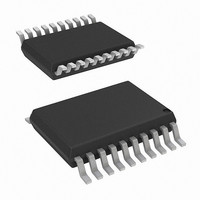
ISOLAT DGTL 2.5KVRMS 4CH 20SSOP
Manufacturer
Analog Devices Inc
Series
iCoupler®r
Datasheet
1.EVAL-ADUM3471EBZ.pdf
(32 pages)
Specifications of ADUM3472CRSZ
Operating Temperature
-40°C ~ 105°C
Inputs - Side 1/side 2
2/2
Number Of Channels
4
Isolation Rating
2500Vrms
Voltage - Supply
3.3V, 5V
Data Rate
25Mbps
Propagation Delay
60ns
Output Type
Logic
Package / Case
20-SSOP (0.200", 5.30mm Width)
No. Of Channels
4
Supply Current
33mA
Supply Voltage Range
3V To 3.6V, 4.5V To 5.5V
Digital Ic Case Style
SSOP
No. Of Pins
20
Operating Temperature Range
-40°C To +105°C
Rohs Compliant
Yes
Lead Free Status / RoHS Status
Lead free / RoHS Compliant
Available stocks
Company
Part Number
Manufacturer
Quantity
Price
Company:

Part Number:
ADUM3472CRSZ
Manufacturer:
Analog Devices Inc
Quantity:
135


ADuM3470/ADuM3471/ADuM3472/ADuM3473/ADuM3474
Parameter
AC SPECIFICATIONS
1
2
3
4
The contributions of supply current values for all four channels are combined at identical data rates.
The V
proportional to the data rate. Additional supply current associated with an individual channel operating at a given data rate can be calculated as described in the
Power Consumption
The power demands of the quiescent operation of the data channels was not separated from the power supply section. Efficiency includes the quiescent power
consumed by the I/O channels as part of the internal power consumption.
This current is available for driving external loads at the V
representing the maximum dynamic load conditions. Refer to the Power C
ADuM347xARWZ
ADuM347xCRWZ
Logic High Output Voltages
Logic Low Output Voltages
Minimum Pulse Width
Maximum Data Rate
Propagation Delay
Pulse Width Distortion, |t
Propagation Delay Skew
Channel-to-Channel Matching
Minimum Pulse Width
Maximum Data Rate
Propagation Delay
Pulse Width Distortion, |t
Propagation Delay Skew
Channel-to-Channel Matching,
Channel-to-Channel Matching,
Output Rise/Fall Time (10% to 90%)
Common-Mode Transient Immunity
Common-Mode Transient Immunity
Refresh Rate
ISO
Change vs. Temperature
Codirectional Channels
Opposing Directional Channels
at Logic High Output
at Logic Low Output
supply current is available for external use when all data rates are below 2 Mbps. At data rates above 2 Mbps, the data I/O channels draw additional current
section. The dynamic I/O channel load must be treated as an external load and included in the V
PLH
PLH
− t
− t
PHL
PHL
|
|
Symbol
V
V
V
V
PW
t
PWD
t
t
PW
t
PWD
t
t
t
t
|CM
|CM
f
r
PHL
PSK
PSKCD
PHL
PSK
PSKCD
PSKOD
R
OAH
OCH
OAL
OCL
/t
, t
, t
F
, V
, V
H
L
, V
, V
|
/t
PLH
PLH
|
ISO
OBL
ODL
ODH
PSKOD
OBH
output. All channels are simultaneously driven at a maximum data rate of 25 Mbps with full capacitive load
,
,
Min
V
V
30
25
25
1
25
CC
CC
− 0.3, V
− 0.5, V
Rev. 0 | Page 10 of 32
onsumption
ISO
ISO
− 0.3
− 0.3
section for calculation of available current at less than the maximum data rate.
Typ
5.0
4.8
0.0
0.0
55
45
5
2.5
35
35
1.0
Max
0.1
0.4
1000
100
40
50
50
40
60
6
15
6
15
Unit
V
V
V
V
ns
Mbps
ns
ns
ns
ns
ns
Mbps
ns
ns
ps/°C
ns
ns
ns
ns
kV/μs
kV/μs
Mbps
ISO
power budget.
Test Conditions/Comments
I
I
I
I
C
C
C
C
C
C
C
C
C
C
C
C
C
C
C
V
transient magnitude = 800 V
V
transient magnitude = 800 V
Ox
Ox
Ox
Ox
L
L
L
L
L
L
L
L
L
L
L
L
L
L
L
Ix
Ix
= 15 pF, CMOS signal levels
= 15 pF, CMOS signal levels
= 15 pF, CMOS signal levels
= 15 pF, CMOS signal levels
= 15 pF, CMOS signal levels
= 15 pF, CMOS signal levels
= 15 pF, CMOS signal levels
= 15 pF, CMOS signal levels
= 15 pF, CMOS signal levels
= 15 pF, CMOS signal levels
= 15 pF, CMOS signal levels
= 15 pF, CMOS signal levels
= 15 pF, CMOS signal levels
= 15 pF, CMOS signal levels
= 15 pF, CMOS signal levels
= −20 μA, V
= −4 mA, V
= 20 μA, V
= 4 mA, V
= V
= 0 V, V = 1000 V,
DD
or V
Ix
ISO
Ix
Ix
= V
Ix
= V
, V
= V
= V
CM
IxL
IxL
IxH
IxH
= 1000 V,
Related parts for ADUM3472CRSZ
Image
Part Number
Description
Manufacturer
Datasheet
Request
R

Part Number:
Description:
±1.7g Dual-Axis IMEMS Accelerometer Evaluation Board
Manufacturer:
Analog Devices Inc
Datasheet:

Part Number:
Description:
Inertial Sensor Evaluation System
Manufacturer:
Analog Devices Inc
Datasheet:
Part Number:
Description:
Manufacturer:
Analog Devices Inc
Datasheet:
Part Number:
Description:
Manufacturer:
Analog Devices Inc
Datasheet:
Part Number:
Description:
Manufacturer:
Analog Devices Inc
Datasheet:
Part Number:
Description:
Manufacturer:
Analog Devices Inc
Datasheet:
Part Number:
Description:
Manufacturer:
Analog Devices Inc
Datasheet:
Part Number:
Description:
Manufacturer:
Analog Devices Inc
Datasheet:
Part Number:
Description:
Manufacturer:
Analog Devices Inc
Datasheet:
Part Number:
Description:
Manufacturer:
Analog Devices Inc
Datasheet:
Part Number:
Description:
Manufacturer:
Analog Devices Inc
Datasheet:
Part Number:
Description:
Manufacturer:
Analog Devices Inc
Datasheet:
Part Number:
Description:
Manufacturer:
Analog Devices Inc
Datasheet: