MT9M413C36STM Aptina LLC, MT9M413C36STM Datasheet - Page 14
MT9M413C36STM
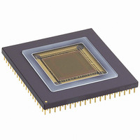
Manufacturer Part Number
MT9M413C36STM
Description
SENSOR IMAGE MONO CMOS 280-PGA
Manufacturer
Aptina LLC
Type
CMOS Imagingr
Specifications of MT9M413C36STM
Pixel Size
12µm x 12µm
Active Pixel Array
1280H x 1024V
Frames Per Second
500
Voltage - Supply
3.3V
Package / Case
280-PGA
Sensor Image Color Type
Monochrome
Sensor Image Size
1280x1024Pixels
Operating Supply Voltage (min)
3V
Operating Supply Voltage (max)
3.6V
Operating Temp Range
-5C to 60C
Package Type
CPGA
Operating Temperature Classification
Commercial
Mounting
Through Hole
Pin Count
280
Lead Free Status / RoHS Status
Contains lead / RoHS non-compliant
Other names
557-1153


Table 3:
09005aef806807ca
MT9M413C36STC.fm - Ver. 3.0 1/04 EN
PIN NUMBER(S)
E4
C2
A1
F5
B2
L3
L2
F1
J4, N15, J16
H3, H18, T18
K2
J3
L1
G18
H16
H15
F18
G17
F17
E18
G15
F16
D18
L5
K4
H2
J5
G3
Pin Description (Continued)
SIGNAL NAME
DATA95
DATA96
DATA97
DATA98
DATA99
CAL_DONE_N
CAL_STRT_N
DARK_OFF_EN_N
VDD
DGND
LD_SHFT_N
DATA_READ_EN_N
LRST_N
ROW_ADDR [9:0]
ROW_ADDR0
ROW_ADDR1
ROW_ADDR2
ROW_ADDR3
ROW_ADDR4
ROW_ADDR5
ROW_ADDR6
ROW_ADDR7
ROW_ADDR8
ROW_ADDR9
ROW_DONE_N
ROW_STRT_N
STANDBY_N
PIXEL_CLK_OUT
SYSCLK
FUNCTION
A two-clock cycle-wide active-low pulse that indicates the ADC has
completed its calibration operation.
Starts the calibration process for the ADC. This is a two- clock cycle-
wide active-low pulse.
A low input enables common mode dark offset to all pixels. The
value of the offset is defined by VREF3 and VCLAMP3. Subtracts a
fixed offset pre-ADC. Signal is pulled up on-chip.
Power supply for core digital circuitry.
Ground for core digital circuitry.
An active-low envelope signal that places the recently converted
row of data into output register for out put, enables the sense amps
and resets the column counter.
An active-low envelope signal that enables the column counter and
causes the ten 10-bit output ports to be updated with data on the
rising edge of the system clock. Column counter skips data when
this input is high.
Global logic reset function (asynchronous). Active-low pulse.
10-bit bus (0 to 1023, bottom to top) that controls which pixel row is
being processed or read out. An asychronous (unclocked) digital
input. Bit 9 is the MSB.
A two-cycle-wide pulse that indicates that processing of the
currently addressed row has been completed.
Starts ADC conversion of the pixel row (defined by the row address)
content. A two-clock cycle-wide active-low pulse.
A low input sets the sensor in a low power mode. (Allow 1
microsecond before calibrating, after coming out of this mode).
Signal is pulled up on-chip.
Data synchronous output. User may prefer to use this pin as data
clock instead of SYSCLK.
Clock input for entire chip. Maximum design frequency is 66 MHz
(50%, ±5%, duty cycle).
1.3-MEGAPIXEL CMOS ACTIVE-PIXEL
14
Micron Technology, Inc., reserves the right to change products or specifications without notice.
DIGITAL IMAGE SENSOR
©2004 Micron Technology, Inc. All rights reserved.
Related parts for MT9M413C36STM
Image
Part Number
Description
Manufacturer
Datasheet
Request
R

Part Number:
Description:
SENSOR IMAGE VGA COLOR CMOS PLCC
Manufacturer:
Aptina LLC
Datasheet:

Part Number:
Description:
IC SENSOR IMAGE COLOR 48CLCC
Manufacturer:
Aptina LLC
Datasheet:

Part Number:
Description:
SENSOR IMAGE 1.3MP CMOS 48-CLCC
Manufacturer:
Aptina LLC
Datasheet:

Part Number:
Description:
SENSOR IMAGE 2MP CMOS 48-CLCC
Manufacturer:
Aptina LLC
Datasheet:

Part Number:
Description:
SENSOR IMAGE VGA MONO 52IBGA
Manufacturer:
Aptina LLC
Datasheet:

Part Number:
Description:
SENSOR IMAGE VGA COLOR 48CLCC
Manufacturer:
Aptina LLC
Datasheet:

Part Number:
Description:
SENSOR IMAGE COLOR CMOS 48-PLCC
Manufacturer:
Aptina LLC
Datasheet:

Part Number:
Description:
KIT HEAD BOARD FOR MT9P031
Manufacturer:
Aptina LLC
Datasheet:

Part Number:
Description:
KIT HEAD BOARD FOR MT9D131
Manufacturer:
Aptina LLC
Datasheet:

Part Number:
Description:
KIT HEAD BOARD FOR MT9P031
Manufacturer:
Aptina LLC
Datasheet:
Part Number:
Description:
SENSOR IMAGE VGA COLOR CMOS PLCC
Manufacturer:
Aptina LLC
Datasheet:
Part Number:
Description:
IC SENSOR IMAGE COLOR 48CLCC
Manufacturer:
Aptina LLC
Datasheet:
Part Number:
Description:
SENSOR IMAGE 2MP CMOS 48-CLCC
Manufacturer:
Aptina LLC
Datasheet:
