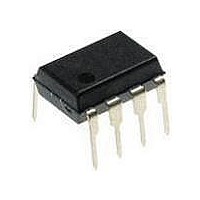
TISP61060P-S Bourns Inc., TISP61060P-S Datasheet - Page 9

TISP61060P-S
Manufacturer Part Number
TISP61060P-S
Description
Sidacs
Manufacturer
Bourns Inc.
Datasheet
1.TISP61060P-S.pdf
(15 pages)
Specifications of TISP61060P-S
Mounting Style
Through Hole
Package / Case
PDIP-8
Lead Free Status / RoHS Status
Lead free / RoHS Compliant
However, often the supply is generated from a switching mode power supply or the SLIC supply feed has a series diode which blocks reverse
(charging) current flow to the battery. In these cases the supply can only sink current in the direction shown by the I
Unless the SLIC current, I
The maximum average value of I
the switching (I
the LB1201AB, it is recommended that the supply should be able to absorb 700 mA of “wrong way” current. If the supply cannot absorb the
current then a shunt breakdown diode is recommended to provided a path for the gate current to ground (D2 in Figure 2). High power diodes
are expensive, so diode D2 is usually low power, purposely selected to fail under this a.c. condition and protect the SLIC.
The TISP61060 improves on the original IC based design in three ways, Figure 5. First, the thin lateral IC structure has been changed to a
vertical power device structure for increased area efficiency and greater energy capability. Second, the series gate diodes have been changed
to transistor buffers. The maximum current injected into the gate supply is then reduced by the transistors gain factor (H
current from the positive voltage diode conduction has been diverted to the gate terminal which subtracts from the normal gate current. In
most cases, this allows any previously used SLIC supply rail shunt protection diode to be removed. Although the SLIC supply is taken to a
terminal that is internally connected to transistor bases, the terminal is still designated as the gate terminal, G.
Figure 6 shows the high impedance a.c. waveforms for the TISP61060. As the TISP61060 replaces the IC based protector’s gate diode with a
transistor, the peak gate current is reduced by over 50 times. In addition there is a compensating negative gate current flow during diode
conduction. The TISP61060 has the maximum value of peak gate current specified and so allows for a designer to design for limit conditions.
Most IC protectors do not specify this parameter. Figure 7 shows the improvement due to the TISP61060. These plots show the full cycle
average gate current against rms a.c. voltage. The IC based protector has a substantial positive gate current which will always charge the
SLIC supply, possibly causing an overvoltage. The TISP61060 has a negative gate current and so cannot overvoltage the SLIC.
SEPTEMBER 1995 — REVISED MARCH 2006
Specifications are subject to change without notice.
Customers should verify actual device performance in their specific applications.
AC Protection Performance (continued)
TISP61060 Buffered Gate Protector
TISP61060 Gated Protector Series
S
) value, see Figure 4. The average current is maximized under high source impedance conditions (e.g. 600 Ω). In the case of
-100
-200
-300
-10
-20
-30
-40
-50
-60
300
200
100
10
0
0
0
0
SLIC
, is equal or greater than I
Figure 4. IC Protector High Impedance Power Cross Clipping Wave Forms
V
G
G
occurs when the thyristor only clips the voltage and the peak cathode current is just beginning to approach
5
5
G
the value of V
I
K
Time - ms
Time - ms
BAT
10
10
will increase, possibly to a level which causes destruction of the SLIC.
V
K
15
15
I
G
BAT
arrow in Figure 2.
FE
20
20
). Third, some
-20
-40
-60
-80
-100
100
80
60
40
20
0
AI6XAH


