SI3585DV-T1-E3 Vishay, SI3585DV-T1-E3 Datasheet
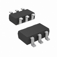
MOSFET N/P-CH 20V 2A/1.5A 6-TSOP

SI3585DV-T1-E3

Manufacturer Part Number
SI3585DV-T1-E3
Description
MOSFET N/P-CH 20V 2A/1.5A 6-TSOP
Manufacturer
Vishay
Series
TrenchFET®r

Specifications of SI3585DV-T1-E3

Transistor Polarity
N and P-Channel
Fet Type
N and P-Channel
Fet Feature
Logic Level Gate
Rds On (max) @ Id, Vgs
125 mOhm @ 2.4A, 4.5V
Drain To Source Voltage (vdss)
20V
Current - Continuous Drain (id) @ 25° C
2A, 1.5A
Vgs(th) (max) @ Id
600mV @ 250µA
Gate Charge (qg) @ Vgs
3.2nC @ 4.5V
Power - Max
830mW
Mounting Type
Surface Mount
Package / Case
6-TSOP
Minimum Operating Temperature
- 55 C
Configuration
Dual
Resistance Drain-source Rds (on)
0.125 Ohm @ 4.5 V @ N Channel
Drain-source Breakdown Voltage
20 V
Gate-source Breakdown Voltage
+/- 12 V
Continuous Drain Current
2 A
Power Dissipation
830 mW
Maximum Operating Temperature
+ 150 C
Mounting Style
SMD/SMT
Continuous Drain Current Id
19A
Drain Source Voltage Vds
20V
On Resistance Rds(on)
200mohm
Rds(on) Test Voltage Vgs
4.5V
Power Dissipation Pd
1.15W
Lead Free Status / RoHS Status
Lead free / RoHS Compliant
Lead Free Status / RoHS Status
Lead free / RoHS Compliant, Lead free / RoHS Compliant
Other names
SI3585DV-T1-E3TR

Available stocks

Company
Part Number
Manufacturer
Quantity
Price
Part Number:
SI3585DV-T1-E3
Manufacturer:
Vishay/Siliconix
Quantity:
26 955
Part Number:
SI3585DV-T1-E3
Manufacturer:
VISHAY/威世
Quantity:
20 000
Company:
Part Number:
SI3585DV-T1-E3
Quantity:
70 000
Notes
a.
Document Number: 71184
S-03512—Rev. B, 04-Apr-01
Drain-Source Voltage
Gate-Source Voltage
Continuous Drain Current (T
Pulsed Drain Current
Continuous Source Current (Diode Conduction)
Maximum Power Dissipation
Operating Junction and Storage Temperature Range
Maximum Junction-to-Ambient
Maximum Junction-to-Foot (Drain)
Surface Mounted on 1” x 1” FR4 Board.
N-Channel
P-Channel
3 mm
G1
G2
S2
Parameter
Parameter
V
DS
J
a
–20
20
= 150_C)
a
1
2
3
Top View
(V)
TSOP-6
2.85 mm
N- and P-Channel 20-V (D-S) MOSFET
_
a
6
5
4
Steady State
Steady State
t v 10 sec
T
T
T
T
a
A
A
A
A
= 25_C
= 70_C
= 25_C
= 70_C
0.200 @ V
0.340 @ V
0.125 @ V
0.200 @ V
D1
S1
D2
r
DS(on)
GS
GS
GS
GS
Symbol
Symbol
T
(W)
R
R
= –4.5 V
= –2.5 V
= 4.5 V
= 2.5 V
J
V
V
I
P
, T
thJA
thJF
DM
I
I
GS
DS
D
S
D
stg
_
G
10 secs
1
Typ
1.05
1.15
0.59
130
N-Channel MOSFET
2.4
1.7
93
75
N-Channel
N-Channel
I
D
–1.8
–1.2
D
S
"12
2.4
1.8
1
1
20
(A)
8
Steady State
Max
110
150
0.75
0.83
0.53
90
2.0
1.4
–55 to 150
10 secs
Typ
130
–1.05
93
75
–1.8
–1.3
1.15
0.59
G
2
P-Channel
P-Channel MOSFET
P-Channel
Vishay Siliconix
"12
–20
–7
Steady State
S
D
2
2
Max
150
110
–0.75
90
Si3585DV
–1.5
–1.2
0.83
0.53
www.vishay.com
Unit
_C/W
C/W
Unit
_C
W
V
A
1

Related parts for SI3585DV-T1-E3

SI3585DV-T1-E3 Summary of contents

Page 1

... 1. 25_C 1. 70_C 0. stg N-Channel Typ Symbol 93 R thJA 130 R 75 thJF Si3585DV Vishay Siliconix P-Channel MOSFET P-Channel 10 secs Steady State –20 "12 2.0 –1.8 –1.5 1.4 –1.3 –1.2 –7 0.75 –1.05 –0.75 0.83 1.15 0.83 0.53 0.59 0.53 –55 to 150 ...

Page 2

... Si3585DV Vishay Siliconix _ Parameter Symbol Static Gate Threshold Voltage Gate-Body Leakage Zero Gate Voltage Drain Current a On-State Drain Current a Drain-Source On-State Resistance a Forward Transconductance a Diode Forward Voltage b Dynamic Total Gate Charge Gate-Source Charge Gate-Drain Charge Turn-On Delay Time Rise Time Turn-Off Delay Time ...

Page 3

... Q – Total Gate Charge (nC) g Document Number: 71184 S-03512—Rev. B, 04-Apr- 300 250 200 150 100 2.0 2.5 Si3585DV Vishay Siliconix Transfer Characteristics –55_C C 8 25_C 0.0 0.5 1.0 1.5 2.0 2.5 3.0 V – Gate-to-Source Voltage (V) GS Capacitance ...

Page 4

... Si3585DV Vishay Siliconix Source-Drain Diode Forward Voltage 150_C 25_C J 0.1 0.00 0.3 0.6 0.9 V – Source-to-Drain Voltage (V) SD Threshold Voltage 0.4 = 250 0.2 –0.0 –0.2 –0.4 –0.6 –50 – – Temperature (_C) J Normalized Thermal Transient Impedance, Junction-to-Ambient 2 1 Duty Cycle = 0.5 ...

Page 5

... I – Drain Current (A) D Document Number: 71184 S-03512—Rev. B, 04-Apr-01 _ – Square Wave Pulse Duration (sec Si3585DV Vishay Siliconix –1 1 Transfer Characteristics –55_C C 6 25_C 0.0 0.5 1.0 1.5 2.0 2.5 3.0 V – Gate-to-Source Voltage (V) GS Capacitance 450 ...

Page 6

... Si3585DV Vishay Siliconix Gate Charge 4 2 3.6 2.7 1.8 0.9 0.0 0.0 0.6 1.2 1.8 Q – Total Gate Charge (nC) g Source-Drain Diode Forward Voltage 150_C 0.1 0.00 0.3 0.6 0.9 V – Source-to-Drain Voltage (V) SD Threshold Voltage 0.6 = 250 0.4 0.2 0.0 – ...

Page 7

... Single Pulse 0.01 –4 – Document Number: 71184 S-03512—Rev. B, 04-Apr-01 _ –2 – Square Wave Pulse Duration (sec) –2 – Square Wave Pulse Duration (sec) Si3585DV Vishay Siliconix Notes Duty Cycle Per Unit Base = R = 87_C/W thJA ( – ...

Page 8

... Vishay disclaims any and all liability arising out of the use or application of any product described herein or of any information provided herein to the maximum extent permitted by law. The product specifications do not expand or otherwise modify Vishay’ ...

Related keywords