SI3585DV-T1-E3 Vishay, SI3585DV-T1-E3 Datasheet - Page 2
SI3585DV-T1-E3
Manufacturer Part Number
SI3585DV-T1-E3
Description
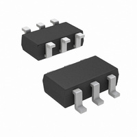
MOSFET N/P-CH 20V 2A/1.5A 6-TSOP
Manufacturer
Vishay
Series
TrenchFET®r
Datasheets
1.SI3585DV-T1-E3.pdf
(8 pages)
2.SI3585DV-T1-E3.pdf
(5 pages)
3.SI3585DV-T1-E3.pdf
(8 pages)
Specifications of SI3585DV-T1-E3
Transistor Polarity
N and P-Channel
Fet Type
N and P-Channel
Fet Feature
Logic Level Gate
Rds On (max) @ Id, Vgs
125 mOhm @ 2.4A, 4.5V
Drain To Source Voltage (vdss)
20V
Current - Continuous Drain (id) @ 25° C
2A, 1.5A
Vgs(th) (max) @ Id
600mV @ 250µA
Gate Charge (qg) @ Vgs
3.2nC @ 4.5V
Power - Max
830mW
Mounting Type
Surface Mount
Package / Case
6-TSOP
Minimum Operating Temperature
- 55 C
Configuration
Dual
Resistance Drain-source Rds (on)
0.125 Ohm @ 4.5 V @ N Channel
Drain-source Breakdown Voltage
20 V
Gate-source Breakdown Voltage
+/- 12 V
Continuous Drain Current
2 A
Power Dissipation
830 mW
Maximum Operating Temperature
+ 150 C
Mounting Style
SMD/SMT
Continuous Drain Current Id
19A
Drain Source Voltage Vds
20V
On Resistance Rds(on)
200mohm
Rds(on) Test Voltage Vgs
4.5V
Power Dissipation Pd
1.15W
Lead Free Status / RoHS Status
Lead free / RoHS Compliant
Lead Free Status / RoHS Status
Lead free / RoHS Compliant, Lead free / RoHS Compliant
Other names
SI3585DV-T1-E3TR
Available stocks
Company
Part Number
Manufacturer
Quantity
Price
Company:

Part Number:
SI3585DV-T1-E3
Manufacturer:
Vishay/Siliconix
Quantity:
26 955
Part Number:
SI3585DV-T1-E3
Manufacturer:
VISHAY/威世
Quantity:
20 000


SPICE Device Model Si3585DV
Notes
a. Pulse test; pulse width ≤ 300 µs, duty cycle ≤ 2.
b. Guaranteed by design, not subject to production testing.
2
Vishay Siliconix
www.vishay.com
SPECIFICATIONS (T
Static
Gate Threshold Voltage
On-State Drain Current
Drain-Source On-State Resistance
Forward Transconductance
Diode Forward Voltage
Dynamic
Total Gate Charge
Gate-Source Charge
Gate-Drain Charge
Turn-On Delay Time
Rise Time
Turn-Off Delay Time
Fall Time
Source-Drain Reverse Recovery Time
b
Parameter
a
a
a
J
= 25°C UNLESS OTHERWISE NOTED)
a
Symbol
V
r
I
DS(on)
t
t
V
Q
D(on)
Q
GS(th)
d(on)
d(off)
g
Q
t
t
t
SD
rr
fs
gs
gd
r
f
g
V
DS
V
I
D
I
DS
D
= −10 V, V
≅ −1 A, V
I
I
S
≅ 1 A, V
S
= 10 V, V
V
V
V
= −1.05 A, di/dt = 100 A/µs
V
V
= 1.05 A, di/dt = 100 A/µs
V
I
V
V
V
DS
V
GS
GS
I
S
DS
V
V
S
DD
GS
DS
DS
GS
DS
= −1.05 A, V
DD
DS
= 1.05 A, V
≤ −5 V, V
= −4.5 V, I
= −2.5 V, I
= V
= 2.5 V, I
= −10 V, R
= V
≥ 5 V, V
= 4.5 V, I
= −5 V, I
=10V, R
= 5 V, I
N-Channel
N-Channel
GEN
GEN
P-Channel
P-Channel
Test Condition
GS
GS
GS
GS
, I
= 4.5 V, R
= −4.5 V, R
, I
= −4.5 V, I
= 4.5 V, I
D
D
GS
GS
D
D
= −250 µA
= 250 µA
L
D
D
D
D
GS
= 2.4 A
= −1.8A
GS
L
= − 4.5 V
= 10 Ω
= 4.5 V
= 2.4 A
= −1.8 A
= −1.2 A
= 1.8 A
= 10 Ω
= 0 V
= 0 V
D
G
D
G
= 2.4 A
= 6 Ω
= −1.8 A
= 6 Ω
N-Ch
N-Ch
N-Ch
N-Ch
N-Ch
N-Ch
N-Ch
N-Ch
N-Ch
N-Ch
N-Ch
N-Ch
N-Ch
N-Ch
P-Ch
P-Ch
P-Ch
P-Ch
P-Ch
P-Ch
P-Ch
P-Ch
P-Ch
P-Ch
P-Ch
P-Ch
P-Ch
P-Ch
Simulated
Data
0.116
0.179
0.153
0.250
−0.78
0.79
1.1
1.1
3.6
1.8
2.5
0.3
0.4
0.4
0.6
19
14
10
10
13
24
52
26
27
20
5
8
7
S-50836Rev. B, 16-May-05
Measured
Document Number: 71760
Data
0.100
0.160
0.160
0.280
−0.83
0.80
3.6
2.1
2.7
0.3
0.4
0.4
0.6
10
11
30
34
14
19
24
30
20
5
6
Unit
nC
ns
Ω
V
A
S
V
Related parts for SI3585DV-T1-E3
Image
Part Number
Description
Manufacturer
Datasheet
Request
R

Part Number:
Description:
MOSFET N/P-CH 20V 6-TSOP
Manufacturer:
Vishay
Datasheet:

Part Number:
Description:
MOSFET 20V 2.4/1.8A
Manufacturer:
Vishay/Siliconix
Datasheet:

Part Number:
Description:
357-036-542-201 CARDEDGE 36POS DL .156 BLK LOPRO
Manufacturer:
Vishay
Datasheet:
Part Number:
Description:
357-036-542-201 CARDEDGE 36POS DL .156 BLK LOPRO
Manufacturer:
Vishay
Datasheet:
Part Number:
Description:
357-036-542-201 CARDEDGE 36POS DL .156 BLK LOPRO
Manufacturer:
Vishay
Datasheet:
Part Number:
Description:
357-036-542-201 CARDEDGE 36POS DL .156 BLK LOPRO
Manufacturer:
Vishay
Datasheet:
Part Number:
Description:
357-036-542-201 CARDEDGE 36POS DL .156 BLK LOPRO
Manufacturer:
Vishay
Datasheet:
Part Number:
Description:
357-036-542-201 CARDEDGE 36POS DL .156 BLK LOPRO
Manufacturer:
Vishay
Datasheet:
Part Number:
Description:
357-036-542-201 CARDEDGE 36POS DL .156 BLK LOPRO
Manufacturer:
Vishay
Datasheet:
Part Number:
Description:
357-036-542-201 CARDEDGE 36POS DL .156 BLK LOPRO
Manufacturer:
Vishay
Datasheet:
Part Number:
Description:
357-036-542-201 CARDEDGE 36POS DL .156 BLK LOPRO
Manufacturer:
Vishay
Datasheet:
Part Number:
Description:
357-036-542-201 CARDEDGE 36POS DL .156 BLK LOPRO
Manufacturer:
Vishay
Datasheet:
Part Number:
Description:
357-036-542-201 CARDEDGE 36POS DL .156 BLK LOPRO
Manufacturer:
Vishay
Datasheet:
Part Number:
Description:
357-036-542-201 CARDEDGE 36POS DL .156 BLK LOPRO
Manufacturer:
Vishay
Datasheet:
Part Number:
Description:
357-036-542-201 CARDEDGE 36POS DL .156 BLK LOPRO
Manufacturer:
Vishay
Datasheet: