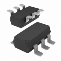
NTGD4167CT1G ON Semiconductor, NTGD4167CT1G Datasheet - Page 4

NTGD4167CT1G
Manufacturer Part Number
NTGD4167CT1G
Description
MOSFET N/P-CH 30V DUAL 6-TSOP
Manufacturer
ON Semiconductor
Datasheet
1.NTGD4167CT1G.pdf
(10 pages)
Specifications of NTGD4167CT1G
Fet Type
N and P-Channel
Fet Feature
Logic Level Gate
Rds On (max) @ Id, Vgs
90 mOhm @ 2.6A, 4.5V
Drain To Source Voltage (vdss)
30V
Current - Continuous Drain (id) @ 25° C
2.6A, 1.9A
Vgs(th) (max) @ Id
1.5V @ 250µA
Gate Charge (qg) @ Vgs
5.5nC @ 4.5V
Input Capacitance (ciss) @ Vds
295pF @ 15V
Power - Max
900mW
Mounting Type
Surface Mount
Package / Case
SC-74-6
Configuration
Dual
Transistor Polarity
N and P-Channel
Drain-source Breakdown Voltage
30 V
Gate-source Breakdown Voltage
+/- 12 V
Continuous Drain Current
2.2 A
Power Dissipation
1100 mW
Maximum Operating Temperature
+ 150 C
Mounting Style
SMD/SMT
Minimum Operating Temperature
- 55 C
Lead Free Status / RoHS Status
Lead free / RoHS Compliant
Available stocks
Company
Part Number
Manufacturer
Quantity
Price
Company:
Part Number:
NTGD4167CT1G
Manufacturer:
ON Semiconductor
Quantity:
4 800
Company:
Part Number:
NTGD4167CT1G
Manufacturer:
ON
Quantity:
30 000
Part Number:
NTGD4167CT1G
Manufacturer:
ON/安森美
Quantity:
20 000
0.20
0.18
0.16
0.14
0.12
0.10
0.08
0.06
0.04
0.02
9.0
8.0
7.0
6.0
5.0
4.0
3.0
2.0
1.0
1.6
1.5
1.4
1.3
1.2
1.1
1.0
0.9
0.8
0.7
0.6
0
0
0
1.0
−50
I
V
D
Figure 3. On−Region vs. Gate−To−Source
GS
0.5
Figure 5. On−Resistance Variation with
= 2.6 A
1.5
−25
Figure 1. On−Region Characteristics
2.5 V
V
= 4.5 V
DS
T
1.0
, DRAIN−TO−SOURCE VOLTAGE (V)
J
V
, JUNCTION TEMPERATURE (°C)
2.0
GS
3.5 V
0
V
1.5
= 4.5 V
GS
, GATE VOLTAGE (V)
I
D
2.5
25
Temperature
2.0
= 2.6 A
Voltage
2.5
3.0
50
N−CHANNEL TYPICAL CHARACTERISTICS
3.0
3.5
75
3.5
100
4.0
T
T
4.0
J
J
= 25°C
= 25°C
http://onsemi.com
2.0 V
1.5 V
4.5
125
4.5
5.0
5.0
150
4
0.10
0.09
0.08
0.07
0.06
0.05
0.04
0.03
0.02
400
350
300
250
200
150
100
9.0
8.0
7.0
6.0
5.0
4.0
3.0
2.0
1.0
0.0
50
0
0.75
0
0
Figure 4. On−Resistance vs. Drain Current and
V
T
C
DS
J
RSS
1.0
= 25°C
= 5 V
V
1
V
Figure 2. Transfer Characteristics
DS
5
GS
Figure 6. Capacitance Variation
, DRAIN−TO−SOURCE VOLTAGE (V)
2.0
, GATE−TO−SOURCE VOLTAGE (V)
125°C
1.25
I
D
C
, DRAIN CURRENT (A)
3.0
10
ISS
V
V
Temperature
GS
GS
1.5
C
4.0
OSS
= 2.5 V
= 4.5 V
15
5.0
1.75
25°C
−55°C
6.0
20
2
7.0
T
V
f = 1 MHz
J
GS
25
2.25
= 25°C
= 0 V
8.0
2.5
9.0
30


