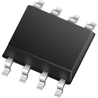
MCP79412T-I/MS Microchip Technology, MCP79412T-I/MS Datasheet - Page 18

MCP79412T-I/MS
Manufacturer Part Number
MCP79412T-I/MS
Description
Real Time Clock I2C GP RTCC 1Kb EE 64B SRAM EUI-64
Manufacturer
Microchip Technology
Series
-r
Type
Clock/Calendarr
Datasheet
1.MCP79412-ISN.pdf
(40 pages)
Specifications of MCP79412T-I/MS
Function
Clock/Calendar
Rtc Memory Size
64 Byte
Maximum Operating Temperature
+ 85 C
Minimum Operating Temperature
- 40 C
Rtc Bus Interface
I2C
Supply Current
1 uA
Features
Alarm, Leap Year, NVSRAM, Square Wave Output, Unique ID
Memory Size
64B
Time Format
HH:MM:SS (12/24 hr)
Date Format
YY-MM-DD-dd
Interface
I²C
Voltage - Supply
1.8 V ~ 5.5 V
Voltage - Supply, Battery
1.3 V ~ 5.5 V
Operating Temperature
-40°C ~ 85°C
Mounting Type
Surface Mount
Package / Case
8-TSSOP, 8-MSOP (0.118", 3.00mm Width)
Lead Free Status / RoHS Status
Lead free / RoHS Compliant
MCP7941X
DS22266C-page 18
5.0
The MCP7941X has both on-board EEPROM memory
and battery-backed SRAM. The SRAM is arranged as
64 x 8 bytes and is retained when the V
removed, provided the V
enabled. The EEPROM is organized as 128 x 8 bytes.
The EEPROM is nonvolatile memory and does not
require the V
5.1
FIGURE 5-1:
FIGURE 5-2:
The 64 bytes of user SRAM are at location 0x20h and
can be accessed during the time when the RTCC is
being internally updated. Upon POR, the SRAM will be
in an undefined state.
Writing to the SRAM and RTCC is accomplished in a
similar way to writing to the EEPROM (as described
later in this document) with the following consider-
ations:
• There is no page. The entire 64 bytes of SRAM or
• The SRAM allows an unlimited number of read/
• The RTCC and SRAM are not accessible when
• The RTCC and SRAM are separate blocks. The
32 bytes of RTCC register can be written in one
command.
write cycles with no cell wear out.
the device is running on the external V
SRAM array may be accessed during an RTCC
update.
ON BOARD MEMORY
SRAM
BUS ACTIVITY
MASTER
SDA LINE
BUS ACTIVITY
BAT
supply for retention.
SRAM/RTCC BYTE WRITE
SRAM/RTCC MULTIPLE BYTE WRITE
BUS ACTIVITY
MASTER
SDA LINE
BUS ACTIVITY
BAT
S
T
A
R
T
S 1 1 0 1
supply is present and
CONTROL
BYTE
1 1 1
BAT
S 1 1 0 1
S
T
A
R
T
CC
0
.
supply is
A
C
K
CONTROL
0
BYTE
ADDRESS
1 1 1
BYTE
0
A
C
K
0
ADDRESS
A
C
K
• Read and write access is limited to either the
• Data written to the RTCC and SRAM are on a per
BYTE
RTCC register block or the SRAM array. The
Address Pointer will rollover to the start of the
addressed block.
byte basis.
Note:
DATA BYTE 0
Entering an address past 0x5F for an
SRAM
MCP7941X
address.
A
C
K
A
C
K
2010-2011 Microchip Technology Inc.
DATA
operation
DATA BYTE N
not
A
C
K
acknowledging
will
S
T
O
P
P
result
A
C
K
S
T
O
P
P
in
the
the


