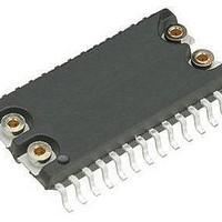
M41T94MH6 STMicroelectronics, M41T94MH6 Datasheet - Page 11

M41T94MH6
Manufacturer Part Number
M41T94MH6
Description
Real Time Clock Serial 512 (64x8)
Manufacturer
STMicroelectronics
Datasheet
1.M41T94MQ6TR.pdf
(41 pages)
Specifications of M41T94MH6
Function
Clock, Calendar, Alarm, Timer Interrupt
Rtc Memory Size
64 B
Supply Voltage (max)
5.5 V
Supply Voltage (min)
2.7 V
Maximum Operating Temperature
+ 85 C
Minimum Operating Temperature
- 40 C
Mounting Style
SMD/SMT
Rtc Bus Interface
Serial
Package / Case
SO-28
Time Format
HH:MM:SS:hh
Lead Free Status / RoHS Status
Lead free / RoHS Compliant
Available stocks
Company
Part Number
Manufacturer
Quantity
Price
Company:
Part Number:
M41T94MH6E
Manufacturer:
ST
Quantity:
740
Company:
Part Number:
M41T94MH6F
Manufacturer:
AOS
Quantity:
26 700
Part Number:
M41T94MH6F
Manufacturer:
ST
Quantity:
20 000
Company:
Part Number:
M41T94MH6TR
Manufacturer:
AD
Quantity:
6 230
M41T94
2
2.1
2.2
2.3
2.4
Signal description
Serial data output (SDO)
The output pin is used to transfer data serially out of the memory. Data is shifted out on the
falling edge of the serial clock.
Serial data input (SDI)
The input pin is used to transfer data serially into the device. Instructions, addresses, and
the data to be written, are each received this way. Input is latched on the rising edge of the
serial clock.
Serial clock (SCL)
The serial clock provides the timing for the serial interface (as shown in
and
on the rising edge of the clock input. The output data on the SDO pin changes state after the
falling edge of the clock input.
The M41T94 can be driven by a microcontroller with its SPI peripheral running in either of
the two following modes:
●
●
For these two modes, input data (SDI) is latched in by the low-to-high transition of clock
SCL, and output data (SDO) is shifted out on the high-to-low transition of SCL (see
on page 10
Chip enable (E)
When E is high, the memory device is deselected, and the SDO output pin is held in its high
impedance state. After power-on, a high-to-low transition on E is required prior to the start of
any operation.
Figure 8 on page
(CPOL, CPHA) = ('0', '0') or
(CPOL, CPHA) = ('1', '1').
and
Figure 6 on page
14). The W/R bit, addresses, or data are latched, from the input pin,
10).
Figure 7 on page 13
Signal description
Table 2
11/41


