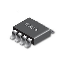
CY2304NZZC-1 Cypress Semiconductor Corp, CY2304NZZC-1 Datasheet - Page 2

CY2304NZZC-1
Manufacturer Part Number
CY2304NZZC-1
Description
Clock Buffer 3.3V 133MHz COM
Manufacturer
Cypress Semiconductor Corp
Datasheet
1.CY2304NZZC-1.pdf
(5 pages)
Specifications of CY2304NZZC-1
Number Of Outputs
4
Max Input Freq
140 MHz
Propagation Delay (max)
5 ns
Supply Voltage (max)
3.6 V
Supply Voltage (min)
3 V
Maximum Operating Temperature
+ 70 C
Minimum Operating Temperature
0 C
Mounting Style
SMD/SMT
Package / Case
TSSOP-8
Lead Free Status / RoHS Status
Lead free / RoHS Compliant
Available stocks
Company
Part Number
Manufacturer
Quantity
Price
Company:
Part Number:
CY2304NZZC-1
Manufacturer:
CY
Quantity:
418
Part Number:
CY2304NZZC-1
Manufacturer:
CYP
Quantity:
20 000
Document #: 38-07099 Rev. *C
Maximum Ratings
Supply Voltage to Ground Potential ........–0.5V to V
DC Input Voltage (Except REF) .............–0.5V to V
DC Input Voltage REF.............................–0.5V to V
Operating Conditions
Electrical Characteristics
Switching Characteristics
Switching Waveforms
Notes:
V
T
C
C
BUF_IN, OUTPUT [1:4] Operating Frequency
t
Duty Cycle Timing
V
V
I
I
V
V
I
1. BUF_IN input has a threshold voltage of V
2. Parameter is guaranteed by design and characterization. It is not 100% tested in production.
3. All parameters specified with loaded outputs.
t
t
t
t
PU
IL
IH
DD
3
4
5
6
A
Parameter
DD
L
IN
IL
IH
OL
OH
Parameter
Parameter
Duty Cycle
Rise Time
Fall Time
Output to Output Skew
Propagation Delay,
BUF_IN Rising Edge to
OUTPUT
1.5V
Input LOW Voltage
Input HIGH Voltage
Input LOW Current
Input HIGH Current
Output LOW Voltage
Output HIGH Voltage
Supply Current
Rising Edge
[2]
Supply Voltage
Operating Temperature (Ambient Temperature)
Load Capacitance
Input Capacitance
Power-up time for all VDD's to reach minimum specified
voltage (power ramps must be monotonic)
[2]
Name
[2]
Description
= t
t
2
2
1.5V
÷ t
[3]
1
DD
[2]
for Commercial and Industrial Temperature Devices
t
1
[1]
[1]
/2.
[2]
[2]
[2]
Measured at 1.5V
Measured between 0.8V and 2.0V
Measured between 0.8V and 2.0V
All outputs equally loaded
Measured at V
1.5V
Description
DD
DD
DD
V
V
I
I
I
I
Unloaded outputs at 66.66 MHz
OL
OL
OH
OH
IN
IN
+0.5V
+0.5V
+0.5V
= 24 mA
= 12 mA
= 0V
= V
= –24 mA
= –12 mA
Description
DD
DD
/2
Test Conditions
Storage Temperature ................................. –65°C to +150°C
Max. Soldering Temperature (10 sec.) ....................... 260°C
Junction Temperature ................................................. 150°C
Static Discharge Voltage
(per MIL-STD-883, Method 3015) ........................... > 2,000V
Min.
40.0
2.5
–
–
–
Min.
0.05
–40
3.0
DC
–
–
Min.
2.0
2.0
2.4
–5
–5
–
–
–
–
Typ.
50.0
3.5
60
–
–
Max.
140
3.6
85
25
50
7
Max.
0.55
0.8
0.8
25
CY2304NZ
–
5
5
–
–
Max.
60.0
1.50
1.50
100
5
Page 2 of 5
MHz
Unit
ms
°C
pF
pF
Unit
V
mA
Unit
µA
µA
V
V
V
V
V
V
ns
ns
ps
ns
%
[+] Feedback


