IRF6710S2TR1PBF International Rectifier, IRF6710S2TR1PBF Datasheet

MOSFET N-CH 25V 12A DIRECTFET

IRF6710S2TR1PBF

Manufacturer Part Number
IRF6710S2TR1PBF
Description
MOSFET N-CH 25V 12A DIRECTFET
Manufacturer
International Rectifier
Series
HEXFET®r
Datasheet

Specifications of IRF6710S2TR1PBF

Fet Type
MOSFET N-Channel, Metal Oxide
Fet Feature
Logic Level Gate
Rds On (max) @ Id, Vgs
5.9 mOhm @ 12A, 10V
Drain To Source Voltage (vdss)
25V
Current - Continuous Drain (id) @ 25° C
12A
Vgs(th) (max) @ Id
2.4V @ 25µA
Gate Charge (qg) @ Vgs
13nC @ 4.5V
Input Capacitance (ciss) @ Vds
1190pF @ 13V
Power - Max
1.8W
Mounting Type
Surface Mount
Package / Case
DirectFET™ Isometric S1
Transistor Polarity
N-Channel
Resistance Drain-source Rds (on)
11.9 mOhms
Drain-source Breakdown Voltage
25 V
Gate-source Breakdown Voltage
20 V
Continuous Drain Current
37 A
Power Dissipation
15 W
Gate Charge Qg
8.8 nC
Lead Free Status / RoHS Status
Lead free / RoHS Compliant
Other names
IRF6710S2TR1PBFTR
l
l
l
l
l
l
l
l
l
Applicable DirectFET Outline and Substrate Outline
Description
The IRF6710S2TRPbF combines the latest HEXFET® Power MOSFET Silicon technology with the advanced DirectFET
achieve improved performance in a package that has the footprint of a MICRO-8 and only 0.7 mm profile. The DirectFET package is
compatible with existing layout geometries used in power applications, PCB assembly equipment and vapor phase, infra-red or convection
soldering techniques, when application note AN-1035 is followed regarding the manufacturing methods and processes. The DirectFET pack-
age allows dual sided cooling to maximize thermal transfer in power systems, improving previous best thermal resistance by 80%.
The IRF6710S2TRPbF has low gate resistance and low charge along with ultra low package inductance providing significant reduction in
switching losses. The reduced losses make this product ideal for high efficiency DC-DC converters that power the latest generation of
processors operating at higher frequencies. The IRF6710S2TRPbF has been optimized for the control FET socket of synchronous buck
operating from 12 volt bus converters.

ƒ
V
V
I
I
I
I
E
I
Absolute Maximum Ratings
www.irf.com
D
D
D
DM
AR
DS
GS
AS
RoHS Compliant
Low Profile (<0.7 mm)
Dual Sided Cooling Compatible 
Ideal for CPU Core DC-DC Converters
100% Rg tested
Click on this section to link to the appropriate technical paper.
Click on this section to link to the DirectFET Website.
Surface mounted on 1 in. square Cu board, steady state.
Ultra Low Package Inductance
Optimized for Control FET Application
@ T
@ T
@ T
Optimized for High Frequency Switching 
Compatible with existing Surface Mount Techniques 
S1
A
A
C
20
15
10
= 25°C
= 70°C
= 25°C
5
0
2.0
Fig 1. Typical On-Resistance vs. Gate Voltage
4.0
S2
V GS , Gate-to-Source Voltage (V)
6.0
Containing No Lead and Halogen Free
Drain-to-Source Voltage
Gate-to-Source Voltage
Continuous Drain Current, V
Pulsed Drain Current
Single Pulse Avalanche Energy
Avalanche Current
8.0 10.0 12.0 14.0 16.0 18.0
SB
T J = 125°C
T J = 25°C
I D = 12A
Ãg
g
Parameter
GS
GS
GS
M2
@ 10V
@ 10V
@ 10V
h

f

M4
25V max ±20V max 4.5mΩ@ 10V 9.0mΩ@ 4.5V
Q
8.8nC
T
Repetitive rating; pulse width limited by max. junction temperature.
Starting T
V
g tot
C
DSS
measured with thermocouple mounted to top (Drain) of part.
12
10
Fig 2. Typical Total Gate Charge vs Gate-to-Source Voltage
8
6
4
2
0
J
0
3.0nC
= 25°C, L = 0.49mH, R
Q
I D = 10A
gd
V
IRF6710S2TR1PbF
4
GS
DirectFET™ Power MOSFET ‚
IRF6710S2TRPbF
L4
Q G Total Gate Charge (nC)
1.3nC
Q
8
gs2
V DS = 20V
VDS= 13V
Max.
100
±20
25
12
10
37
24
10
R
L6
12
DS(on)
8.0nC
G
Q
= 25Ω, I
rr
16
DirectFET™ ISOMETRIC
AS
4.4nC
L8
Q
= 10A.
20
oss
TM
R
packaging to
DS(on)
24
Units
V
mJ
1.8V
03/16/10
V
A
A
gs(th)
1

Related parts for IRF6710S2TR1PBF

IRF6710S2TR1PBF Summary of contents

Page 1

... 25° Fig 2. Typical Total Gate Charge vs Gate-to-Source Voltage „ T measured with thermocouple mounted to top (Drain) of part. C … Repetitive rating; pulse width limited by max. junction temperature. † Starting T = 25° 0.49mH IRF6710S2TRPbF IRF6710S2TR1PbF DirectFET™ Power MOSFET ‚ DS(on) DS(on gs2 rr oss 1 ...

Page 2

Static @ T = 25°C (unless otherwise specified) J Parameter BV Drain-to-Source Breakdown Voltage DSS ∆ΒV /∆T Breakdown Voltage Temp. Coefficient DSS J R Static Drain-to-Source On-Resistance DS(on) V Gate Threshold Voltage GS(th) ∆V /∆T Gate Threshold Voltage Coefficient GS(th) ...

Page 3

Absolute Maximum Ratings 25°C Power Dissipation 70°C Power Dissipation D A Power Dissipation 25° Peak Soldering Temperature P T Operating Junction and J T Storage Temperature ...

Page 4

PULSE WIDTH Tj = 25°C 0.01 0 Drain-to-Source Voltage (V) Fig 4. Typical Output Characteristics 1000 100 175° 25° ...

Page 5

175°C 100 25° -40° 0.1 0.2 0.4 0.6 0 Source-to-Drain Voltage (V) Fig 10. Typical Source-Drain Diode Forward Voltage ...

Page 6

Duty Cycle = Single Pulse 10 0.01 1 0.05 0.10 Allowed avalanche Current vs avalanche 0.1 pulsewidth, tav, assuming ∆Τ 25°C and Tstart = 150°C. 0.01 1.0E-06 1.0E-05 Fig 16. Typical Avalanche Current Vs.Pulsewidth 30 TOP Single ...

Page 7

DUT 0 1K 20K S Fig 18a. Gate Charge Test Circuit D.U 20V 0.01 Ω Fig 19a. Unclamped Inductive Test Circuit ≤ 1 ≤ 0.1 % Fig 20a. Switching Time Test ...

Page 8

D.U.T + ƒ • • - • + ‚ „  • G • • SD • Fig 19. ™ 8 Driver Gate Drive Period P.W. D.U.T. I Waveform SD Reverse Recovery Body Diode Forward Current + D.U.T. ...

Page 9

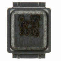
Please see AN-1035 for DirectFET assembly details and stencil and substrate design recommendations DirectFET™ Part Marking www.irf.com DIMENSIONS METRIC IMPERIAL CODE MAX MIN MIN MAX A 4.75 4.85 0.187 0.191 3.95 0.146 B 3.70 0.156 2.85 C 0.108 2.75 ...

Page 10

... DirectFET™ Tape & Reel Dimension (Showing component orientation). NOTE: Controlling dimensions in mm Std reel quantity is 4800 parts. (ordered as IRF6710S2TRPBF). For 1000 parts on 7" reel, order IRF6710S2TR1PBF CODE WORLD HEADQUARTERS: 233 Kansas St., El Segundo, California 90245, USA Tel: (310) 252-7105 10 REEL DIMENSIONS ...

Related keywords