NTHD3101FT1G ON Semiconductor, NTHD3101FT1G Datasheet
NTHD3101FT1G
Specifications of NTHD3101FT1G
Available stocks


Related parts for NTHD3101FT1G

NTHD3101FT1G Summary of contents
Page 1
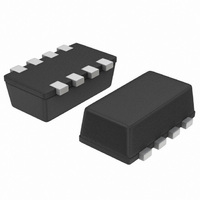
NTHD3101F Power MOSFET and Schottky Diode −20 V, FETKYt, P−Channel, −4.4 A, with 4.1 A Schottky Barrier Diode, ChipFETt Features • Leadless SMD Package Featuring a MOSFET and Schottky Diode • 40% Smaller than TSOP−6 Package • Leadless SMD Package ...
Page 2
THERMAL RESISTANCE RATINGS Parameter Junction−to−Ambient – Steady State (Note 2) Junction−to−Ambient – t ≤ (Note 2) 2. Surface Mounted on FR4 Board using pad size (Cu area = 1.127 oz] including traces). ...
Page 3
TYPICAL P−CHANNEL PERFORMANCE CURVES − −3 − −2 −V , DRAIN−TO−SOURCE VOLTAGE ...
Page 4
TYPICAL P−CHANNEL PERFORMANCE CURVES 1500 ISS 1200 900 600 C RSS 300 −V − GATE−TO−SOURCE OR DRAIN−TO−SOURCE VOLTAGE (VOLTS) Figure 7. Capacitance ...
Page 5
TYPICAL SCHOTTKY PERFORMANCE CURVES 150° 25° −55°C J 0.1 0.20 0.40 0. INSTANTANEOUS FORWARD VOLTAGE (VOLTS) F Figure 11. Typical Forward Voltage 1E− 150°C J 100E−6 ...
Page 6
... DEVICE ORDERING INFORMATION Device NTHD3101FT1 NTHD3101FT1G NTHD3101FT3 NTHD3101FT3G †For information on tape and reel specifications, including part orientation and tape sizes, please refer to our Tape and Reel Packaging Specifications Brochure, BRD8011/D. Package ChipFET ChipFET (Pb−Free) ChipFET ChipFET (Pb−Free) http://onsemi.com 6 † Shipping 3000 / Tape & ...
Page 7
... A 0.457 0.018 *For additional information on our Pb−Free strategy and soldering details, please download the ON Semiconductor Soldering and Mounting Techniques Reference Manual, SOLDERRM/D. ChipFET is a trademark of Vishay Siliconix. FETKY is a registered trademark of International Rectifier Corporation. ON Semiconductor and are registered trademarks of Semiconductor Components Industries, LLC (SCILLC). SCILLC reserves the right to make changes without further notice to any products herein ...