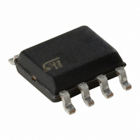
STS4DPFS30L STMicroelectronics, STS4DPFS30L Datasheet - Page 2

STS4DPFS30L
Manufacturer Part Number
STS4DPFS30L
Description
MOSFET P-CH 30V 5A 8-SOIC
Manufacturer
STMicroelectronics
Series
STripFET™r
Datasheet
1.STS4DPFS30L.pdf
(9 pages)
Specifications of STS4DPFS30L
Fet Type
MOSFET P-Channel, Metal Oxide
Fet Feature
Diode (Isolated)
Rds On (max) @ Id, Vgs
55 mOhm @ 2.5A, 10V
Drain To Source Voltage (vdss)
30V
Current - Continuous Drain (id) @ 25° C
5A
Vgs(th) (max) @ Id
2.5V @ 250µA
Gate Charge (qg) @ Vgs
16nC @ 5V
Input Capacitance (ciss) @ Vds
1350pF @ 25V
Power - Max
2.5W
Mounting Type
Surface Mount
Package / Case
8-SOIC (3.9mm Width)
Configuration
Single Dual Drain
Transistor Polarity
P-Channel
Resistance Drain-source Rds (on)
0.045 Ohms
Forward Transconductance Gfs (max / Min)
10 S
Drain-source Breakdown Voltage
- 30 V
Gate-source Breakdown Voltage
+/- 16 V
Continuous Drain Current
4 A
Power Dissipation
2.5 W
Maximum Operating Temperature
+ 150 C
Mounting Style
SMD/SMT
Minimum Operating Temperature
- 55 C
Lead Free Status / RoHS Status
Contains lead / RoHS non-compliant
Other names
497-4397-2
Available stocks
Company
Part Number
Manufacturer
Quantity
Price
STS4DPFS30L
2/9
Table 3: MOSFET Absolute Maximum Ratings
( )
Note: For the P-CHANNEL MOSFET actual polarity of voltages and current has to be reversed
Table 4: Schottky Absolute Maximum Ratings
Table 5: Thermal Data
(*) Mounted on FR-4 board (Steady State)
ELECTRICAL CHARACTERISTICS (T
Table 6: On/Off
Rthj-case Thermal Resistance Junction-case Single Operating
Rthj-amb
V
Symbol
Symbol
Symbol
R
I
V
I
Pulse width limited by safe operating area
(BR)DSS
V
V
F(RMS)
DM
P
I
dv/dt
I
I
I
I
V
I
V
F(AV)
DS(on)
T
RRM
GS(th)
RSM
FSM
DSS
GSS
DGR
RRM
I
I
TOT
T
T
stg
DS
GS
D
D
j
l
( )
Drain-source Voltage (V
Drain-gate Voltage (R
Gate- source Voltage
Drain Current (continuous) at T
Single Operating
Drain Current (continuous) at T
Single Operating
Drain Current (pulsed)
Total Dissipation at T
Operating Junction Temperature
Storage Temperature
Repetitive Peak Reverse Voltage
RMS Forward Current
Average Forward Current
Surge Non Repetitive Forward Current
Repetitive Peak Reverse Current
Non Repetitive Peak Reverse Current
Critical Rate Of Rise Of Reverse Voltage
(*)Thermal Resistance Junction-ambient SCHOTTKY
Maximum Lead Temperature For Soldering Purpose
Drain-source
Breakdown Voltage
Zero Gate Voltage
Drain Current (V
Gate-body Leakage
Current (V
Gate Threshold Voltage
Static Drain-source On
Resistance
Parameter
DS
= 0)
Parameter
GS
= 0)
C
GS
Parameter
= 25°C Single Operating
GS
= 20 k )
I
V
V
V
V
V
V
= 0)
D
DS
DS
GS
DS
GS
GS
= 250 µA, V
= Max Rating
= Max Rating, T
= ± 16V
= 10 V, I
= 4.5 V, I
C
C
= V
CASE
= 25°C
= 100°C
Test Conditions
GS
, I
=25°C UNLESS OTHERWISE SPECIFIED)
D
D
D
= 2.5 A
= 250 µA
= 2.5 A
GS
= 0
TL = 125°C
tp = 10 ms
Sinusoidal
tp = 2 s
F = 1 kHz
tp = 100 s
= 0.5
C
= 125°C
Min.
30
1
-55 to 150
10000
Value
Value
0.045
0.065
± 16
Typ.
100
300
2.5
150
1.6
30
30
20
30
20
75
50
5
4
3
1
1
0.055
0.075
±100
Max
2.5
10
1
°C/W
°C/W
V/ s
Unit
Unit
Unit
°C
°C
°C
W
µA
µA
nA
V
A
A
A
A
A
V
V
V
A
A
A
V
V


