STB40NF10T4 STMicroelectronics, STB40NF10T4 Datasheet - Page 4
STB40NF10T4
Manufacturer Part Number
STB40NF10T4
Description
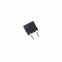
MOSFET N-CH 100V 50A D2PAK
Manufacturer
STMicroelectronics
Series
STripFET™r
Datasheet
1.STB40NF10T4.pdf
(13 pages)
Specifications of STB40NF10T4
Fet Type
MOSFET N-Channel, Metal Oxide
Fet Feature
Logic Level Gate
Rds On (max) @ Id, Vgs
28 mOhm @ 25A, 10V
Drain To Source Voltage (vdss)
100V
Current - Continuous Drain (id) @ 25° C
50A
Vgs(th) (max) @ Id
4V @ 250µA
Gate Charge (qg) @ Vgs
80nC @ 10V
Input Capacitance (ciss) @ Vds
1780pF @ 25V
Power - Max
150W
Mounting Type
Surface Mount
Package / Case
D²Pak, TO-263 (2 leads + tab)
Transistor Polarity
N Channel
Continuous Drain Current Id
40A
Drain Source Voltage Vds
100V
On Resistance Rds(on)
28mohm
Rds(on) Test Voltage Vgs
10V
Threshold Voltage Vgs Typ
1.7V
Rohs Compliant
Yes
Configuration
Single
Resistance Drain-source Rds (on)
0.024 Ohms
Forward Transconductance Gfs (max / Min)
20 S
Drain-source Breakdown Voltage
100 V
Gate-source Breakdown Voltage
+/- 20 V
Continuous Drain Current
50 A
Power Dissipation
150 W
Maximum Operating Temperature
+ 175 C
Mounting Style
SMD/SMT
Minimum Operating Temperature
- 55 C
Lead Free Status / RoHS Status
Lead free / RoHS Compliant
Other names
497-6552-2
STB40NF10T4
STB40NF10T4
Available stocks
Company
Part Number
Manufacturer
Quantity
Price
Company:

Part Number:
STB40NF10T4
Manufacturer:
ST MICROELECTRONICS
Quantity:
30 000


Electrical characteristics
2
4/13
Electrical characteristics
(T
Table 3.
Table 4.
1. Pulsed: Pulse duration = 300 µs, duty cycle 1.5 %.
V
Symbol
Symbol
CASE
R
V
(BR)DSS
g
t
t
I
C
I
C
GS(th)
DS(on)
C
Q
d(on)
d(off)
Q
DSS
GSS
fs
Q
oss
t
t
iss
rss
gs
gd
r
f
(1)
g
=25°C unless otherwise specified)
Forward
transconductance
Input capacitance
Output capacitance
Reverse transfer
capacitance
Turn-on delay time
Rise time
Turn-off delay time
Fall time
Total gate charge
Gate-source charge
Gate-drain charge
Drain-source
breakdown voltage
Zero gate voltage
drain current (V
Gate-body leakage
current (V
Gate threshold voltage
Static drain-source on
resistance
On/off states
Dynamic
Parameter
Parameter
DS
= 0)
GS
= 0)
I
V
V
T
V
V
V
V
V
V
V
R
(see
V
V
(see
D
C
DS
DS
GS
DS
GS
GS
GS
DS
DS
DD
DD
G
= 250µA, V
= 125°C
Test conditions
= 4.7Ω V
Test conditions
= Max rating
= Max rating,
= ± 20V
= V
= 10V, I
= 25V
= 25V, f = 1MHz,
= 0
= 50V, I
= 80V, I
= 10V, R
Figure
Figure
GS
,
, I
I
D
13)
14)
D
GS
D
D
D
G
GS
= 25A
= 25A
= 25A
= 50A,
= 250µA
= 4.7Ω
= 10V
=0
Min.
Min.
100
2
0.024
1780
Typ.
Typ.
60.6
22.8
265
112
2.8
9.6
20
28
63
84
28
0.028
Max.
Max.
±100
80
10
STB40NF10
1
4
Unit
Unit
nC
nC
nC
pF
pF
pF
ns
ns
ns
ns
µA
µA
nA
S
V
V
Ω
Related parts for STB40NF10T4
Image
Part Number
Description
Manufacturer
Datasheet
Request
R


Part Number:
Description:
STMicroelectronics [RIPPLE-CARRY BINARY COUNTER/DIVIDERS]
Manufacturer:
STMicroelectronics
Datasheet:
Part Number:
Description:
STMicroelectronics [LIQUID-CRYSTAL DISPLAY DRIVERS]
Manufacturer:
STMicroelectronics
Datasheet:

Part Number:
Description:
BOARD EVAL FOR MEMS SENSORS
Manufacturer:
STMicroelectronics
Datasheet:
Part Number:
Description:
NPN TRANSISTOR POWER MODULE
Manufacturer:
STMicroelectronics
Datasheet:
Part Number:
Description:
TURBOSWITCH ULTRA-FAST HIGH VOLTAGE DIODE
Manufacturer:
STMicroelectronics
Datasheet:
Part Number:
Description:
Manufacturer:
STMicroelectronics
Datasheet:
Part Number:
Description:
DIODE / SCR MODULE
Manufacturer:
STMicroelectronics
Datasheet:
Part Number:
Description:
DIODE / SCR MODULE
Manufacturer:
STMicroelectronics
Datasheet:
Part Number:
Description:
Search -----> STE16N100
Manufacturer:
STMicroelectronics
Datasheet:
Part Number:
Description:
Search ---> STE53NA50
Manufacturer:
STMicroelectronics
Datasheet:
Part Number:
Description:
NPN Transistor Power Module
Manufacturer:
STMicroelectronics
Datasheet: