ZXMN6A11GTC Diodes Zetex, ZXMN6A11GTC Datasheet
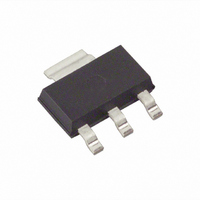
MOSFET N-CHAN 60V SOT223

ZXMN6A11GTC

Manufacturer Part Number
ZXMN6A11GTC
Description
MOSFET N-CHAN 60V SOT223
Manufacturer
Diodes Zetex
Datasheet

Specifications of ZXMN6A11GTC

Fet Type
MOSFET N-Channel, Metal Oxide
Fet Feature
Logic Level Gate
Rds On (max) @ Id, Vgs
120 mOhm @ 2.5A, 10V
Drain To Source Voltage (vdss)
60V
Current - Continuous Drain (id) @ 25° C
3.1A
Vgs(th) (max) @ Id
1V @ 250µA
Gate Charge (qg) @ Vgs
5.7nC @ 10V
Input Capacitance (ciss) @ Vds
330pF @ 40V
Power - Max
2W
Mounting Type
Surface Mount
Package / Case
SOT-223 (3 leads + Tab), SC-73, TO-261
Lead Free Status / RoHS Status
Lead free / RoHS Compliant

Available stocks

Company
Part Number
Manufacturer
Quantity
Price
Part Number:
ZXMN6A11GTC
Manufacturer:
ZETEX/DIODES
Quantity:
20 000
Ordering Information
Marking Information
Product Summary
Description and Applications
This MOSFET has been designed to minimize the on-state resistance
and yet maintain superior switching performance, making it ideal for
high efficiency power management applications.
Notes:
ZXMN6A11G
Document number: DS33556 Rev. 5 - 2
DC-DC converters
Power management functions
Disconnect switches
Motor Control
Uninterrupted power supply
V
ZXMN6A11GTA
(BR)DSS
60V
Product
1. Diodes, Inc. defines “Green” products as those which are RoHS compliant and contain no halogens or antimony compounds; further information
about Diodes Inc.’s “Green” Policy can be found on our website. For packaging details, go to our website.
180mΩ @ V
120mΩ @ V
Top View
SOT223
R
DS(on)
GS
GS
(Note 1)
= 4.5V
= 10V
See below
Marking
T
A
ZXMN
4.4A
3.5A
6A11
= 25°C
I
D
Reel size (inches)
www.diodes.com
60V N-CHANNEL ENHANCEMENT MODE MOSFET
Pin Out - Top
1 of 8
ZXMN = Product Type Marking Code, Line 1
6A11 = Product Type Marking Code, Line 2
7
Features and Benefits
Mechanical Data
Fast switching speed
Low gate drive
Low input capacitance
“Green” component and RoHS compliant (Note 1)
Qualified to AEC-Q101 Standards for High Reliability
Case: SOT223
Case Material: Molded Plastic, “Green” Molding Compound.
UL Flammability Classification Rating 94V-0 (Note 1)
Moisture Sensitivity: Level 1 per J-STD-020
Terminals Connections: See diagram below
Terminals: Finish - Matte Tin annealed over Copper lead frame.
Solderable per MIL-STD-202, Method 208
Weight: 0.112 grams (approximate)
Tape width (mm)
Diodes Incorporated
A Product Line of
12
G
Equivalent Circuit
D
S
Quantity per reel
ZXMN6A11G
1,000
© Diodes Incorporated
October 2010

Related parts for ZXMN6A11GTC

ZXMN6A11GTC Summary of contents

Page 1

Product Summary V R (BR)DSS DS(on) 120mΩ 10V GS 60V 180mΩ 4.5V GS Description and Applications This MOSFET has been designed to minimize the on-state resistance and yet maintain superior switching performance, making it ...

Page 2

Maximum Ratings @T = 25°C unless otherwise specified A Characteristic Drain-Source Voltage Gate-Source Voltage Continuous Drain Current V = 10V GS Pulsed Drain Current V = 10V GS Continuous Source Current (Body Diode) Pulsed Source Current (Body Diode) Thermal Characteristics ...

Page 3

Thermal Characteristics R 10 DS(on) Limited 100m 100ms 10ms T =25°C amb 25mm x 25mm 10m 1oz FR4 1 V Drain-Source Voltage (V) DS Safe Operating Area 60 T =25°C amb 25mm x 25mm 50 1oz FR4 ...

Page 4

Electrical Characteristics @T Characteristic OFF CHARACTERISTICS Drain-Source Breakdown Voltage Zero Gate Voltage Drain Current Gate-Source Leakage ON CHARACTERISTICS Gate Threshold Voltage Static Drain-Source On-Resistance (Note 6) Forward Transconductance (Notes 6 & 7) Diode Forward Voltage (Note 6) Reverse Recovery Time ...

Page 5

Typical Characteristics T = 25° 0.1 0.1 V Drain-Source Voltage (V) DS Output Characteristics 10V 150° 25°C 0 Gate-Source Voltage (V) GS Typical Transfer Characteristics 1 ...

Page 6

Typical Characteristics - continued 500 400 300 C ISS C 200 OSS 100 Drain - Source Voltage (V) DS Capacitance v Drain-Source Voltage Test Circuit Basic gate charge ...

Page 7

Package Outline Dimensions Millimeters DIM Min Max A - 1.80 A1 0.02 0.10 A2 1.55 1.65 b 0.66 0.84 b2 2.90 3.10 C 0.23 0.33 Suggested Pad Layout ZXMN6A11G Document number: DS33556 Rev Inches DIM Min Max ...

Page 8

DIODES INCORPORATED MAKES NO WARRANTY OF ANY KIND, EXPRESS OR IMPLIED, WITH REGARDS TO THIS DOCUMENT, INCLUDING, BUT NOT LIMITED TO, THE IMPLIED WARRANTIES OF MERCHANTABILITY AND FITNESS FOR A PARTICULAR PURPOSE (AND THEIR EQUIVALENTS UNDER THE LAWS OF ANY ...

Related keywords